
The MicroBlaze Micro Controller Syste (MCS) is a soft-core processor that can be customized and placed inside the fabric of your FPGA. The uses of this are limitless.
Requirements:
- LabVIEW 2017
- LabVIEW 2017 FPGA Module
- LabVIEW 2017 FPGA Module Xilinx Compilation Tools for Vivado 2015.4
- Xilinx Software Development Kit version 2015.4
Source Code
Browse the source code online via github by visiting the following link:
To download the source code, clone the entire repository with:
- git clone git@github.com:JohnStratoudakis/LabVIEW_Fpga.git
You can also download a zip file with the entire repository:
What this Guide Accomplishes
This guide shows how to use the version of Xilinx Vivado that is bundled with the “LabVIEW 2017 FPGA Module Xilinx Compilation Tools” to create a Vivado FPGA design that uses a MicroBlaze MCS core, to create and overlay an executable on top of that core using Xilinx SDK 2015.4, and finally how to import this design and to run it on the National Instruments PXIe-6592R High-Speed Serial Instrument.
References for Further Reading
- LabVIEW
- LabVIEW FPGA Module
- National Instruments PXIe-6592R (High-Speed Serial Instrument)
- Xilinx MicroBlaze Micro Controller System
Slide Share version
SlideShare (Opens in new tab)
Video Demonstration of Run
This guide is broken down in to the following sections:
- Section 1 – Vivado – Create MicroBlaze MCS design
- Section 2 – Xilinx SDK – Write a C Program for the MicroBlaze MCS
- Section 3 – Vivado – Add Binary (ELF) to MicroBlaze MCS design
- Section 4 – LabVIEW 2017 – Import design to LabVIEW and run on FPGA
Section 1 – Vivado – Create MicroBlaze MCS Design
Step 1 – Start Vivado 2015.4
If you haven’t set up a shortcut, just run the following batch file:
- C:\NIFPGA\programs\Vivado2015_4\bin\vivado.bat
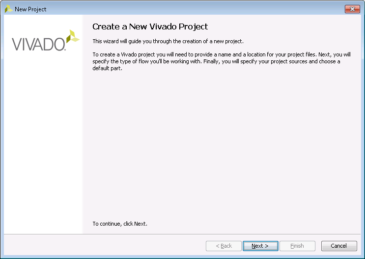
Step 2 – Create a New Project
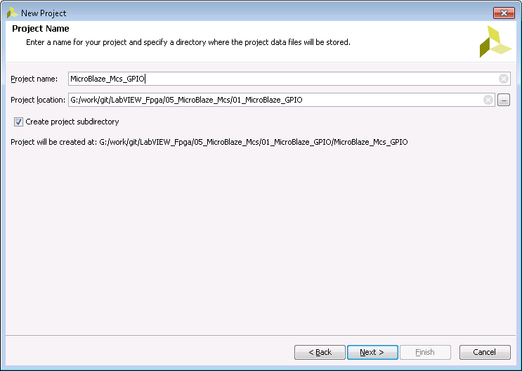
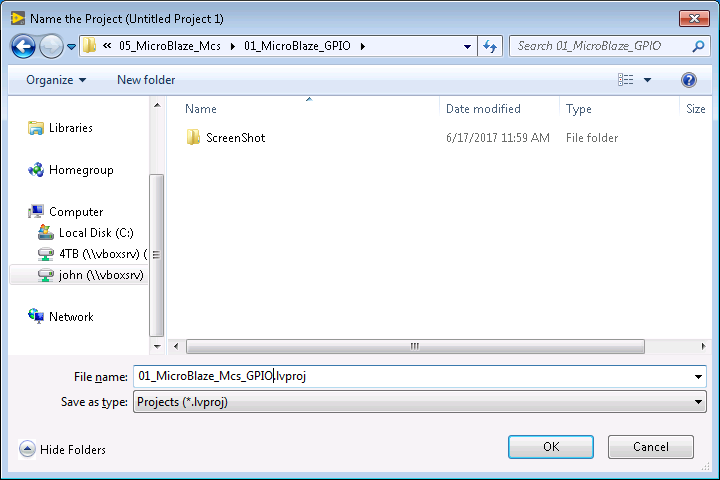
Step 3 – Select Project Location and Project Name
I created my project in the following location: (screenshot is out of date)
- G:/work/git/LabVIEW_Fpga/05_MicroBlaze_Mcs/01_MicroBlaze_MCS_GPIO
I named my project “MicroBlaze_Mcs_GPIO”
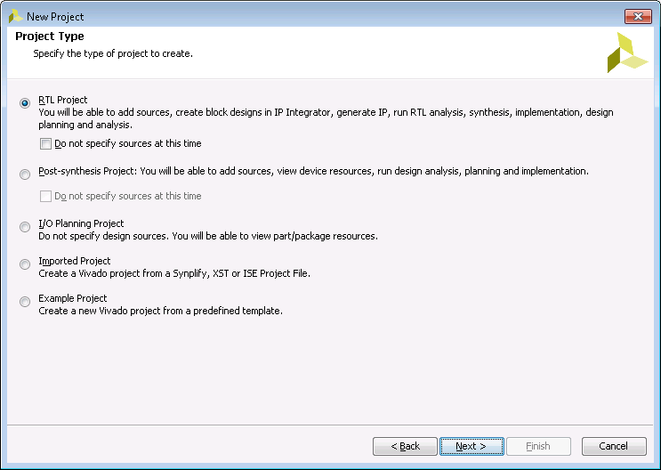
Step 4 – Just click next, I did not set anything here
Step 5 – Make sure the “Target language” is VHDL.
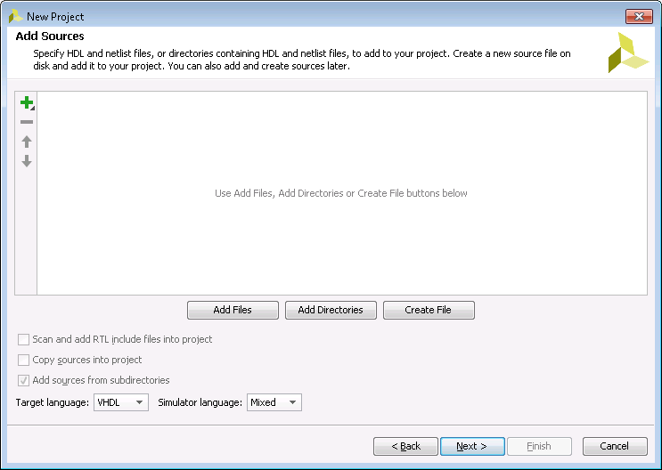
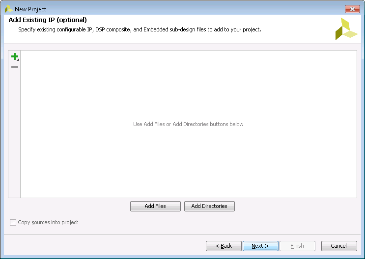
Step 6 – Just click next in the Add Existing IP page
Step 7 – Click next, we are not adding any constraints, nor do we have to in this project.

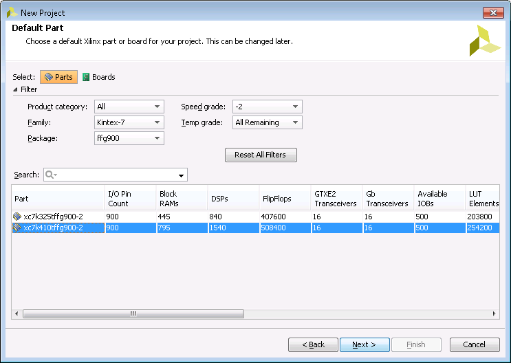
Step 8 – Select the appropriate FPGA part
We are using the PXIe-6592R board for this example and the FPGA has the following specifications:
- Family: Kintex-7
- Speed Grade: -2
- Package: ffg900
- Part #: xc7k410t
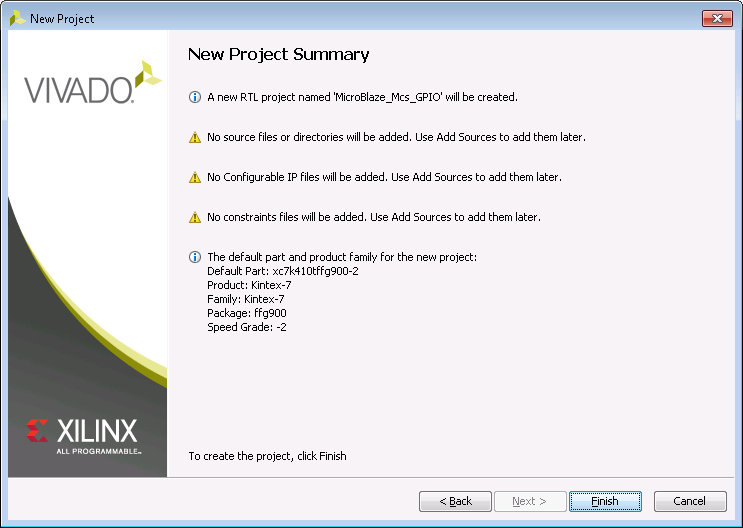
Step 9 – Click finish to create your new project
Step 10 – Here is what the project looks like after creation. Click on the image below for a higher resolution image to appear in a new window.
![]()
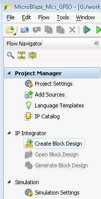
Step 11 – Click “Create Block Design”
Vivado makes it easy to create designs. By clicking on create block design, you can make a design that uses several cores and makes it easy to synthesize, package and to export to an application such as LabVIEW
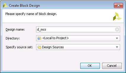
Step 12 – Name the design
I like using the d_ prefix followed by a short description of my design. Since we are using the MicroBlaze MCS, I name my design “d_mcs”
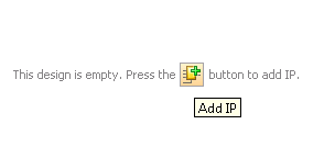
Step 13 – Here is the blank design
![]()
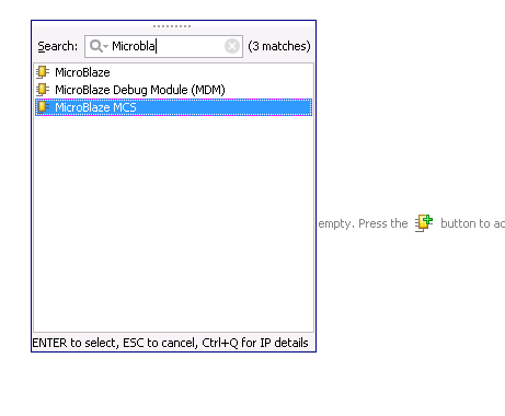
Step 14 – Click the “Add IP” button to get a list of all Xilinx available cores
Step 15 – Make sure you select the “MicroBlaze MCS” and not the “MicroBlaze”
The MicroBlaze core is more customizable and supports more features, I will cover this in a future article.
Step 16 – After adding the MicroBlaze MCS core. Notice that no peripherals have been added, nor has the core been configured.

Step 17 – Right click (away from any terminals) and customize the block.
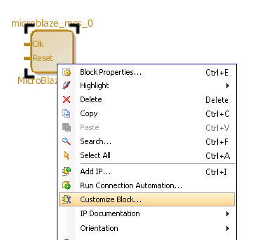
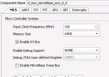
Step 18 – Configure the MicroBlaze MCS core

Step 19 – Set the memory size to 64 KB and enable the IO Bus if you like. I will use the IO Bus in a future article
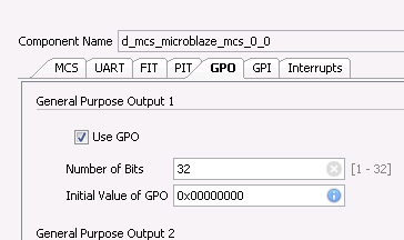
Step 20 – Enable the General Purpose Output (GPO) channel 1, 32 bits is fine.
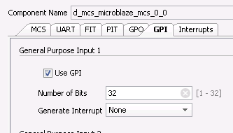
Step 21 – Enable the General Purpose Input (GPI) channel 1, 32 bits is fine.
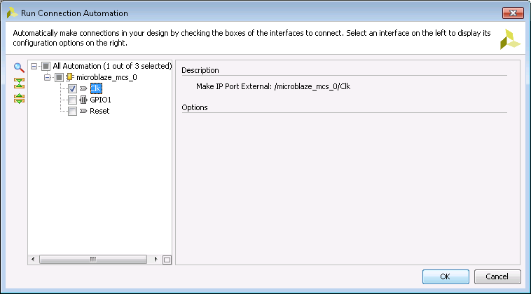
Step 22 – Click on “Run Connection Automation” at the top of the window containing the design. Check the Clk box.
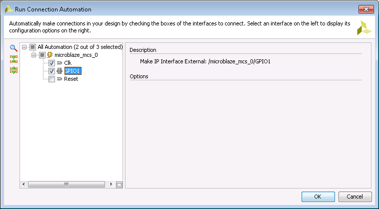
Step 23 – The defaults for GPIO2 should be fine as well.
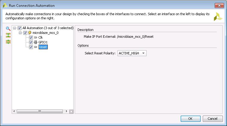
Step 24 – Same for Reset. Note how the Reset Polarity is set to ACTIVE_HIGH. This will not matter for our design, but it will in other cases. i.e. I was dealing with the Arty Artix-7 board, and I had to flip the reset polarity for that board to work.
Step 25 – Now if you enabled the IO Bus, you have to manually make it external. Make sure you right-click and that the cursor becomes pencil-like as shown below.
Step 26 – Click “Make External”
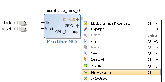
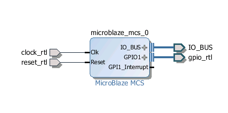
Step 27 – Here is what it looks like after clicking “Make External”
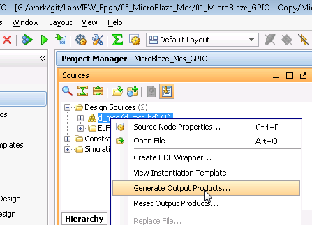
Step 28 – Now go back to the block design and right-click on the design containing the MicroBlaze MCS and select “Generate Output Products”
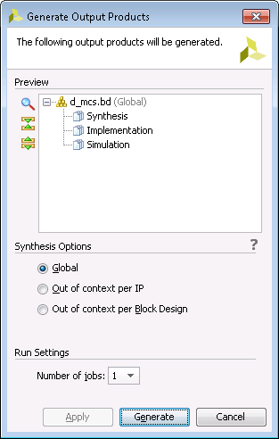
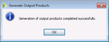
Step 29 – Global should be fine.
Step 30 – When Vivado is finished, you should see the following.
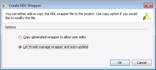
Step 31 – Now right-click on the design and select “Create HDL Wrapper”

Step 32 – Either option should be fine here, but I like having Vivado manage this for me automatically in case I make changes to my block design.
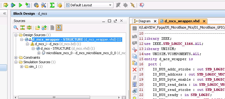
Step 33 – Notice how there is a new VHDL file, that contains an instantiation of everything in our Block Design.

Step 34 – A preview of the contents of the VHDL design wrapper. From LabVIEW we will be importing this wrapper.
Section 2 – Xilinx SDK Write a C program
Step 1 – Now we take a break from Vivado and launch the Xilinx SDK. You can normally export the hardware from Vivado and ask it to launch the SDK, but there is a bug in this version of Vivado (2015.4) that prevents us from doing so only in the case that our design is using the MicroBlaze MCS. Note that this does not apply to designs using the MicroBlaze core.

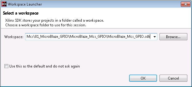
Step 2 – Create a directory named “MicroBlaze_Mcs_GPIO.sdk” as a sub-directory inside the Vivado project directory and set this to be your workspace.
Normally, if you select “File->Export->Hardware”, this directory will automatically be created for you, but remember that the hdf file that will exist in the root directory will not work due to a bug in Vivado 2015.4, so I typically create the directory myself.
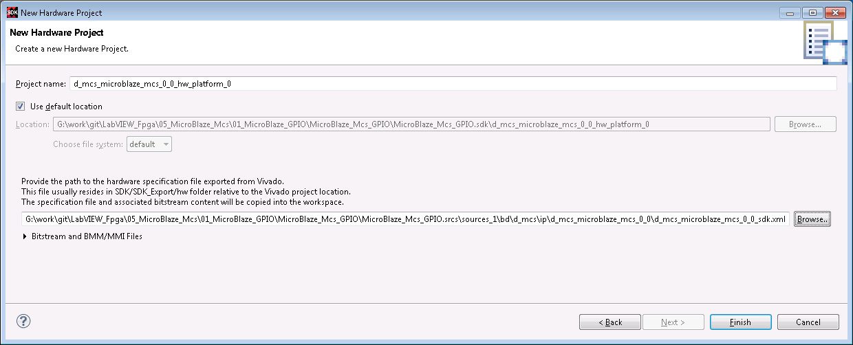
Step 3 – Click “File->New->Other” to get to the New Project Wizard.

Step 4 – Select Hardware Specification.

Step 5 – Click the “Browse” button and add the following file, make sure you select the file ending with “_sdk.xml”
The full path from the root of the Vivado project is as follows:
MicroBlaze_Mcs_GPIO.srcs\sources_1\bd\d_mcs\ip\d_mcs_microblaze_mcs_0_0\d_mcs_microblaze_mcs_0_0_sdk.xml

Step 6 – The default name is okay, just click Finish after selecting the XML file from the step above.
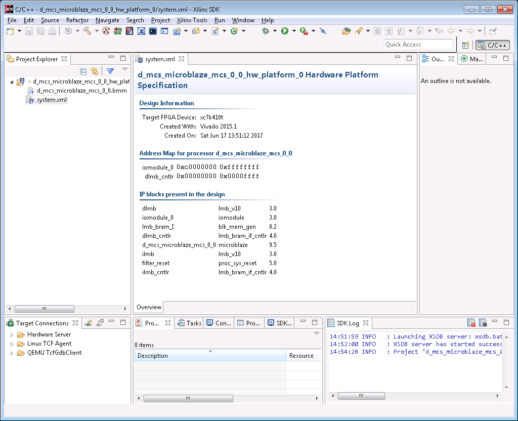
Step 7 – What the new project looks like. Notice the Target FPGA Device and the address map.
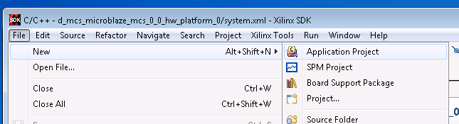
Step 8 – Now create a new Application Project.
Step 9 – Call this project “gpio_rw”, our project will read from GPI-1 and write out of GPO-1.
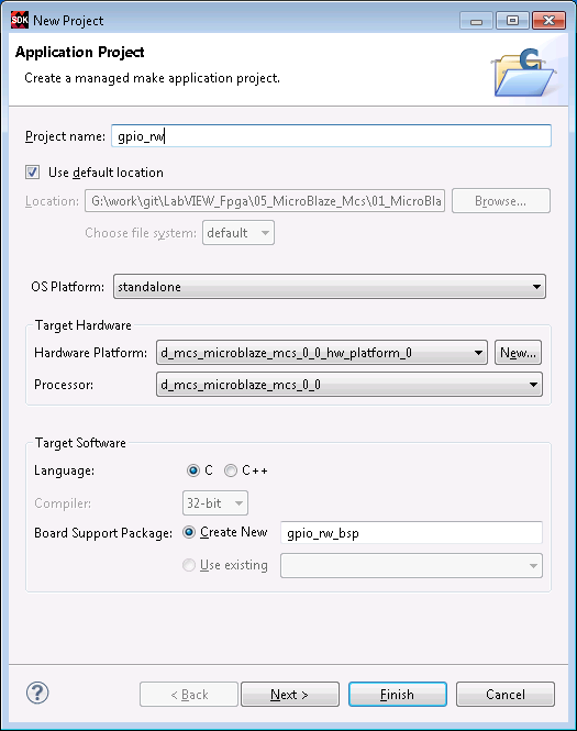
Step 10 – Select Empty Application, I will provide the code that you should insert.
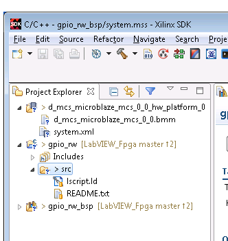
Step 11 – Right click on the “src” directory to create a new C source.
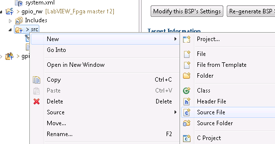
Step 12 – After right-clicking, select “New->Source File”
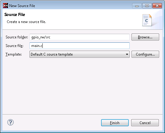
Step 13 – Name this file main.c
Step 14 – Copy and Paste the following source code:
| /* * main.c * * Created on: Jun 17, 2017 * Author: John */#include “xparameters.h” #include “xil_cache.h” #include “xiomodule.h”int main() {Xil_ICacheEnable();Xil_DCacheEnable();print(“—Entering main—\n\r”);{ XIOModule gpioIn_1; XIOModule_Initialize(&gpioIn_1, XPAR_IOMODULE_0_DEVICE_ID); XIOModule_Start(&gpioIn_1); XIOModule gpioOut_1; XIOModule_Initialize(&gpioOut_1, XPAR_IOMODULE_0_DEVICE_ID); XIOModule_Start(&gpioOut_1); u32 gpi_1; while(1) { gpi_1 = XIOModule_DiscreteRead(&gpioIn_1, 1); if(gpi_1 == 0) { gpi_1 = 50; } XIOModule_DiscreteWrite(&gpioOut_1, 1, gpi_1 + gpi_1); } } print(“—Exiting main—\n\r”); Xil_DCacheDisable(); Xil_ICacheDisable(); return 0; } |
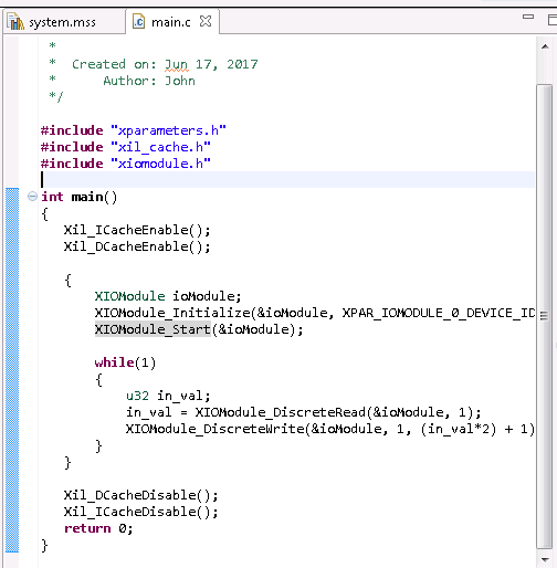
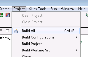
Step 15 – Building should automatically take place when you save the source file. But click “Project->Build All” to confirm this.
Section 3 – Vivado Part 2
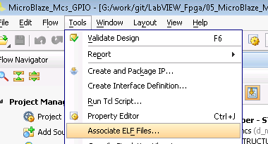
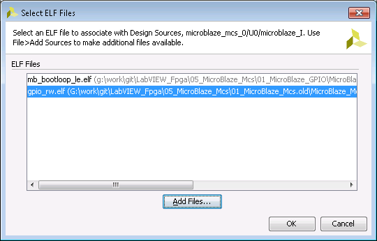
Step 1 – Go back to your Vivado project and select “Tools->Associate ELF Files…”
Step 2 – Click the “…” button next to the elf file, which should be “mb_bootloop_le.elf” for both Design Sources and Simulation Sources.

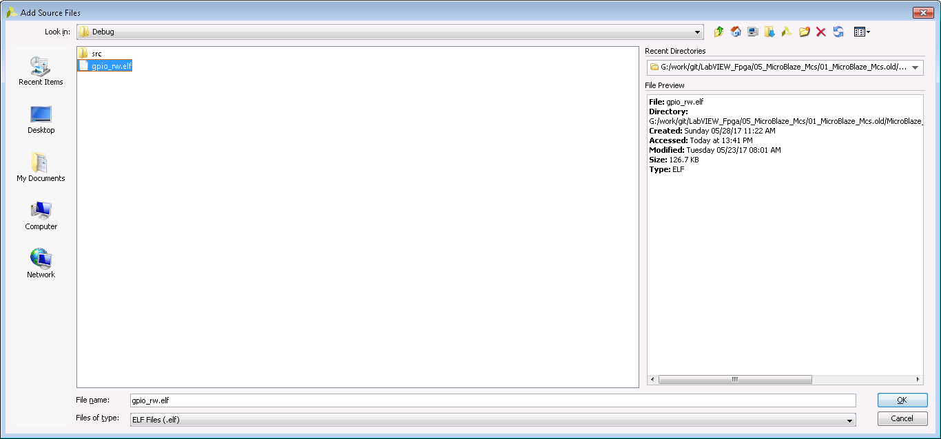
Step 3 – Add your binary, which should be located in the following directory:
MicroBlaze_Mcs_GPIO/MicroBlaze_Mcs_GPIO.sdk/gpio_rw/src/Debug/gpio_rw.elf
Step 4 – Click ok, the new elf file should automatically be selected.
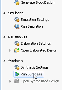
Step 5 – Now run the Synthesis.
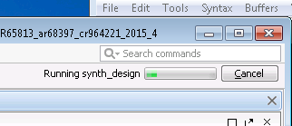
Step 6 – You can verify that synthesis is running by looking at the top-right of the Vivado Window.
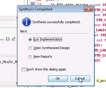
Step 7 – After a couple of minutes when Synthesis finishes, click Cancel, because we do not want to run the implementation. LabVIEW will handle that!
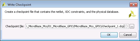
Step 8 – Write a checkpoint by clicking “File->Write Checkpoint”
Note that you must write a Synthesized Checkpoint, which means that you have to have followed the steps above and not have run Implementation. If you run implementation, the checkpoint file will be larger than if you only ran synthesis. In case you made a mistake and implemented your design, simply open the Synthesized design and write a new checkpoint.
Section 4 – LabVIEW 2017
Step 1 – LabVIEW 2017 splash screen. I like the new look.
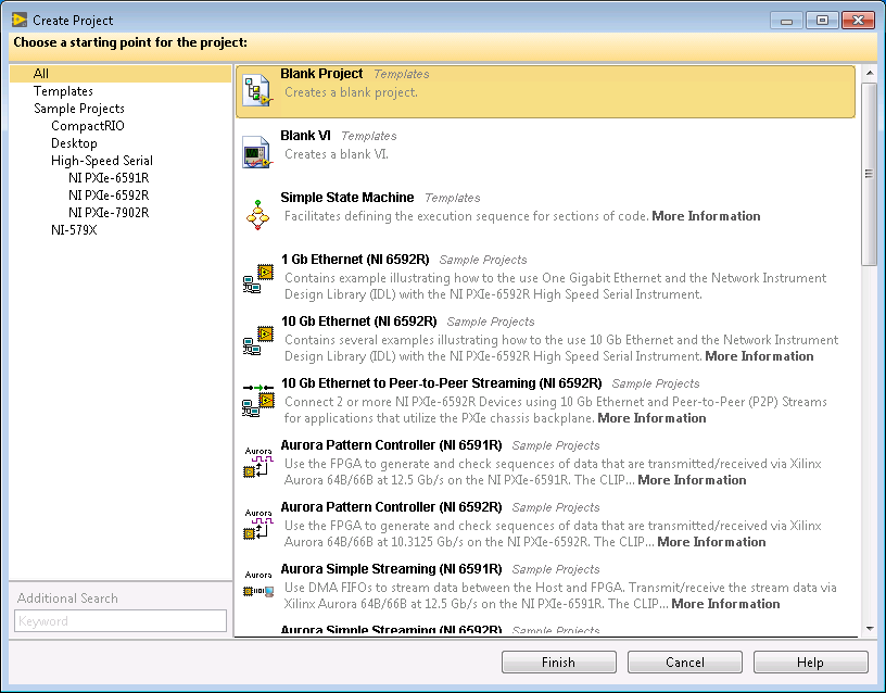
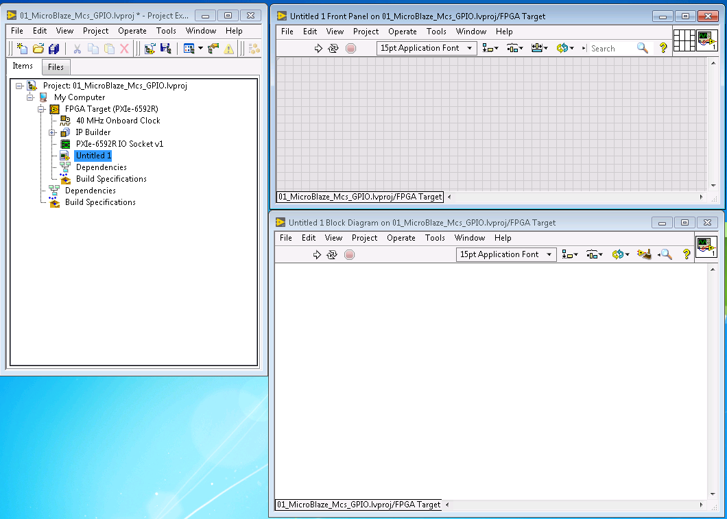
Step 2 – Create a new Project.
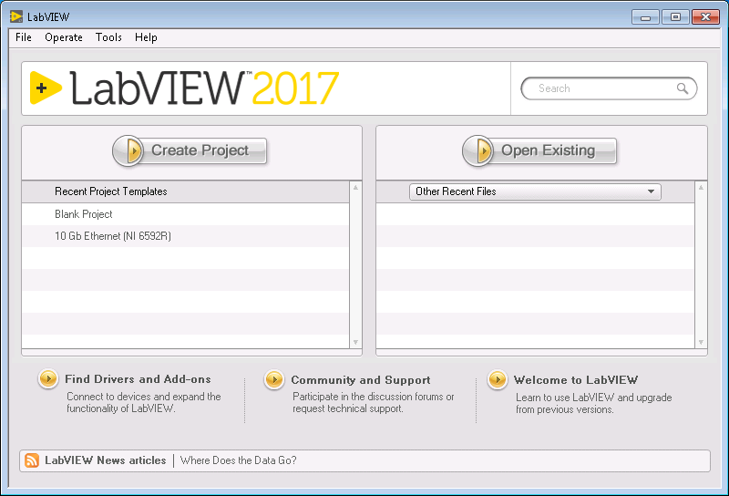
Step 3 – Blank Project is fine.
Step 4 – Here is what an empty project looks like before you save it.
![]()
Step 5 – Add a new target, for this tutorial we are going to be using the PXIe-6592R High-Speed Serial Instrument.
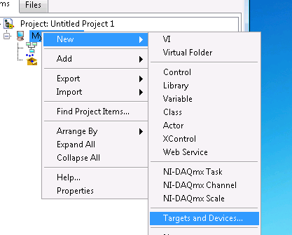
Step 6 – If you do not have live hardware plugged in, select New target or device, if you do, it should show up automatically.

Step 7 – After adding the PXIe-6592R
Step 8 – Click File->Save and save the project.
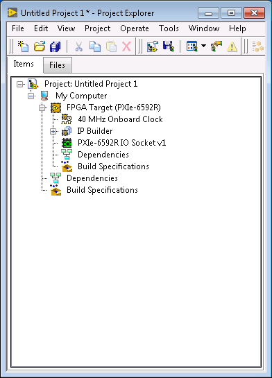
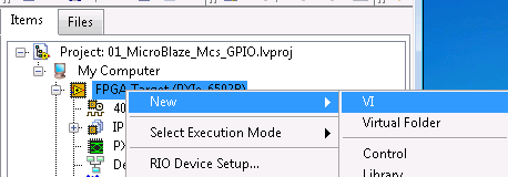
Step 9 – Add a new FPGA-scoped VI. Make sure you right-click on the FPGA-target for this.
Step 10 – I opened the VI and cleaned up the windows and show the block diagram here.
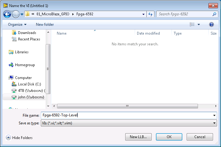
Step 11 – Now click “File->Save” to save the FPGA-scoped VI
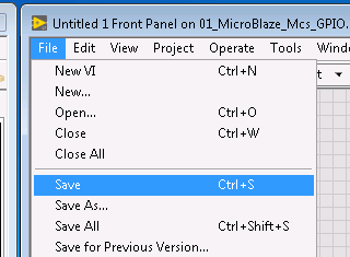
Step 12 – I usually save FPGA-scoped VIs in a sub-directory named after the FPGA target. In this case “Fpga-6592”
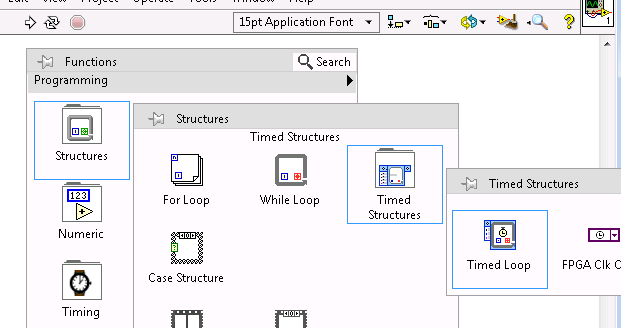
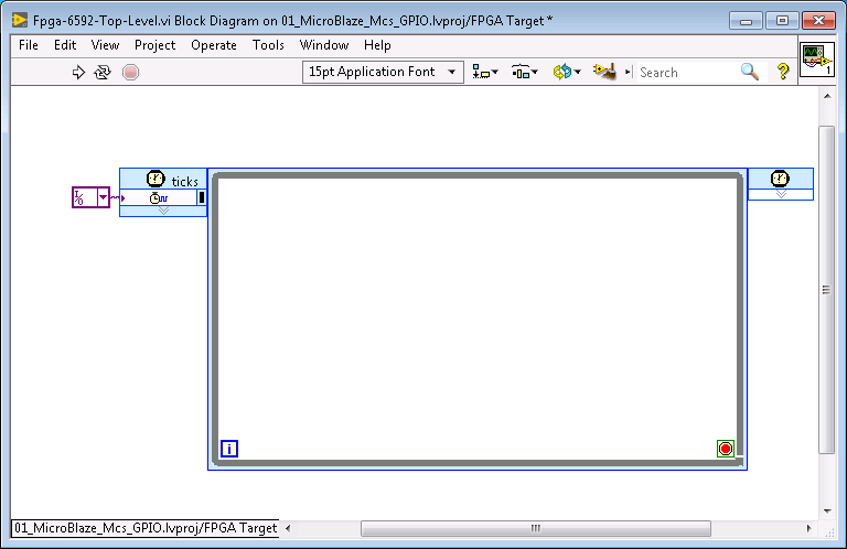
Step 13 – Right-click anywhere in the blank white space and select “Timed Loop” to add a Single-Cycle Timed Loop.
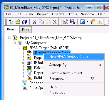
Step 14 – Add a new FPGA clock since the default of 40 MHz is not suitable for our 100 MHz MicroBlaze MCS.
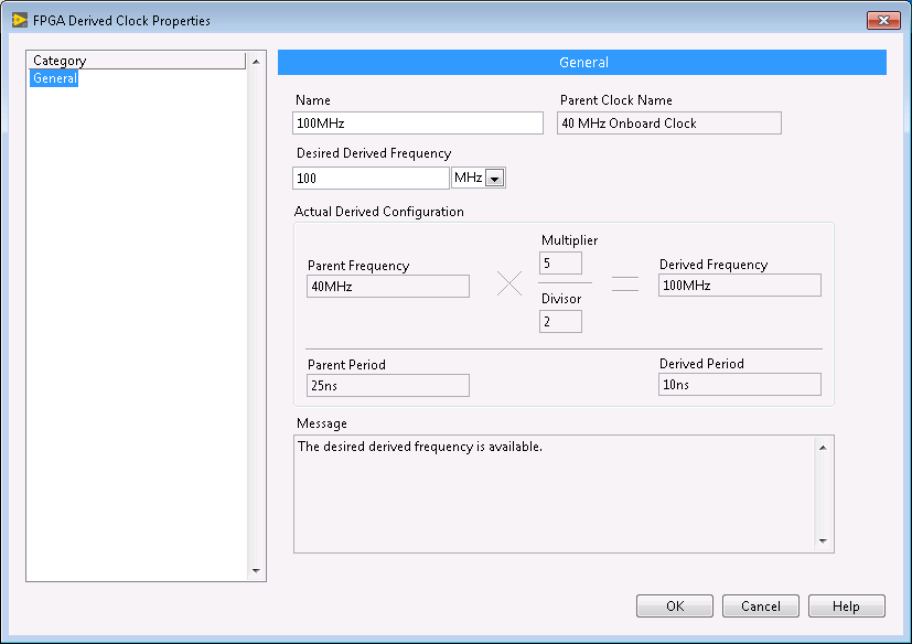
Step 15 – Just type 100 in the “Desired Derived Frequency box and click ok
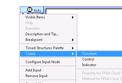
Step 16 – Now right-click on the clock input to the Single-Cycle Timed Loop and select Create->Constant
Step 17 – Here is what the loop looks like before selecting the clock type.
Step 18 – Dropdown should reveal 2 clocks. You select 100 MHz
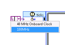
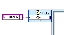
Step 19 – After selecting 100 MHz
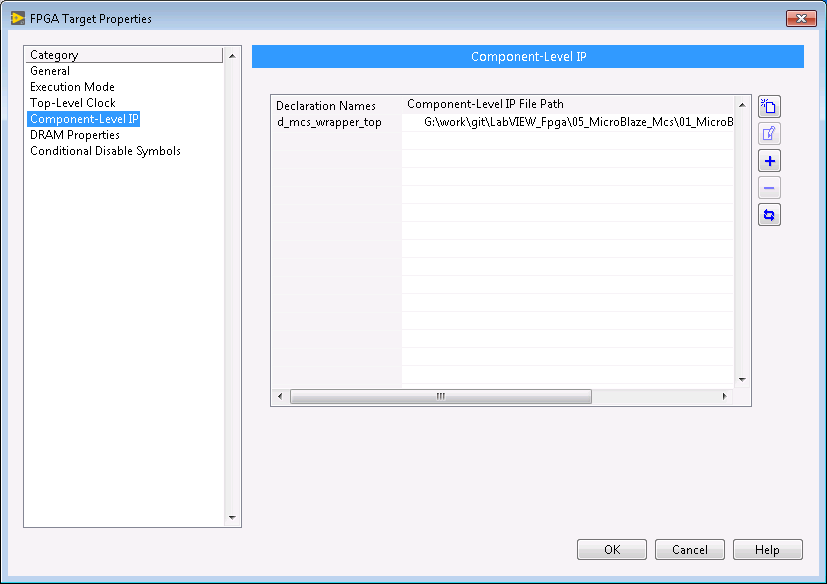
Step 20 – Now to configure the CLIP node. CLIP stands for Component Level IP.
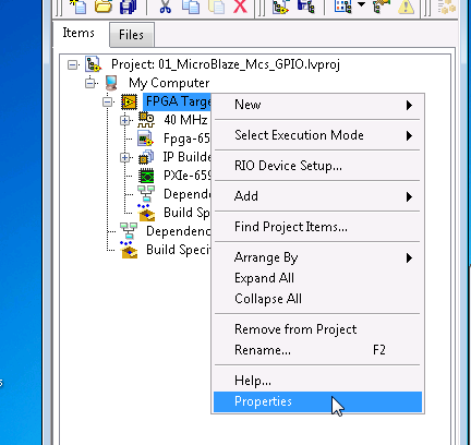
Step 21 – Click Component-Level IP in the left, and then click on the Create File icon on the right.
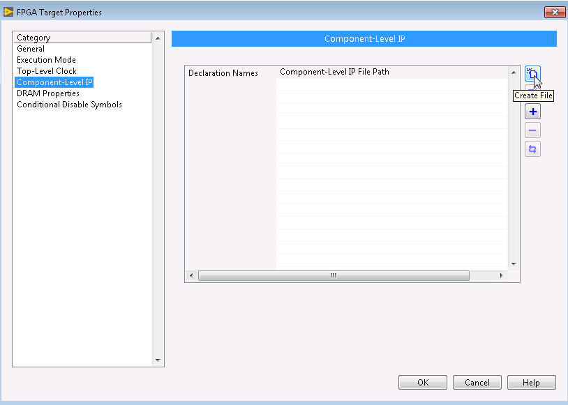
Step 22 – Add the checkpoint dcp file, and the wrapper vhdl file.
The wrapper file can be found here:
I also have a sample checkpoint file, but you ideally want to create this yourself:
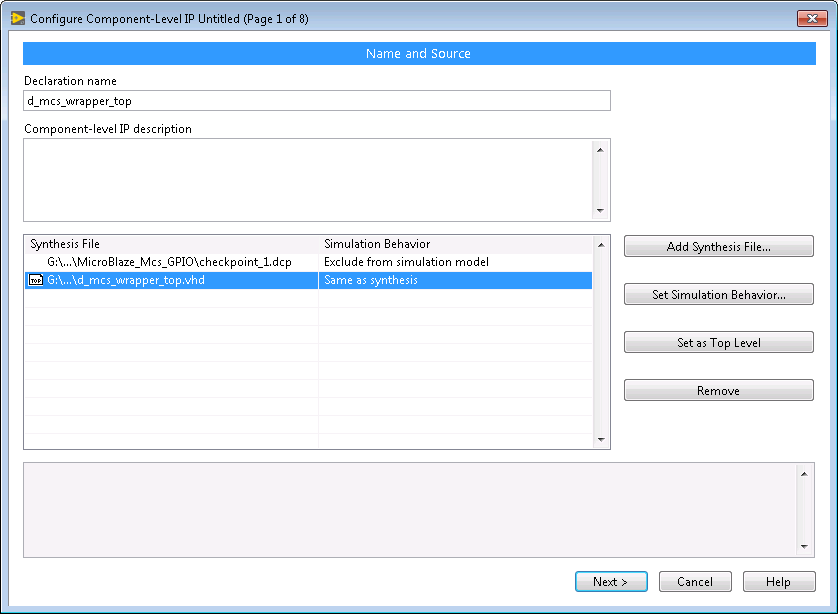
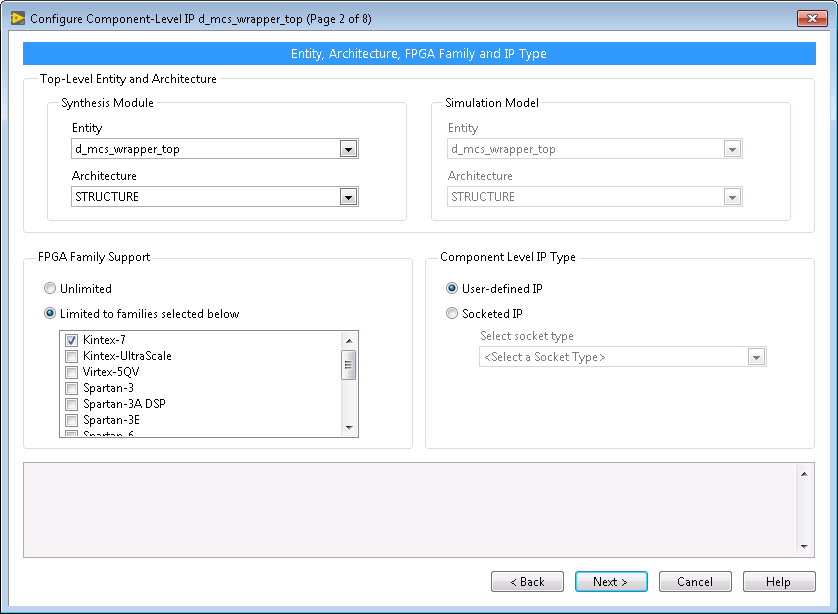
Step 23 – Depending on your target, you may have to limit the device families.
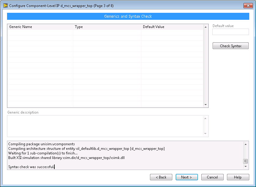
Step 24 – Click Chek Syntax, this requires the Vivado Compilation Tools to be installed in order to work.
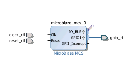
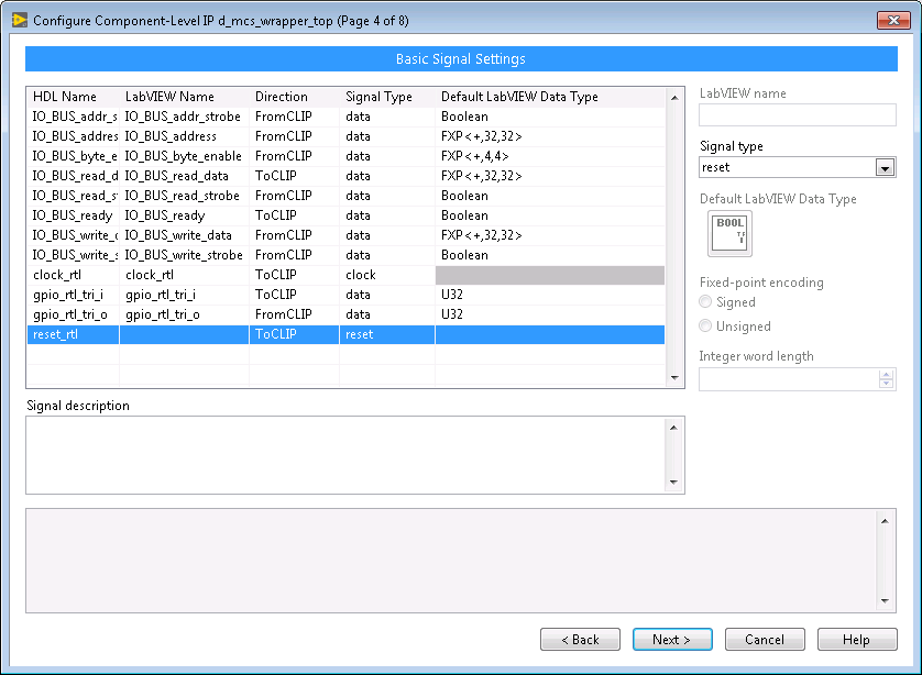
Step 25 – Set the reset_rtl Signal type to be reset, the clock_rtl signal type to be clock, and set the data type for the gpio_rtl_tri_i and gpio_rtl_tri_o to be U32.
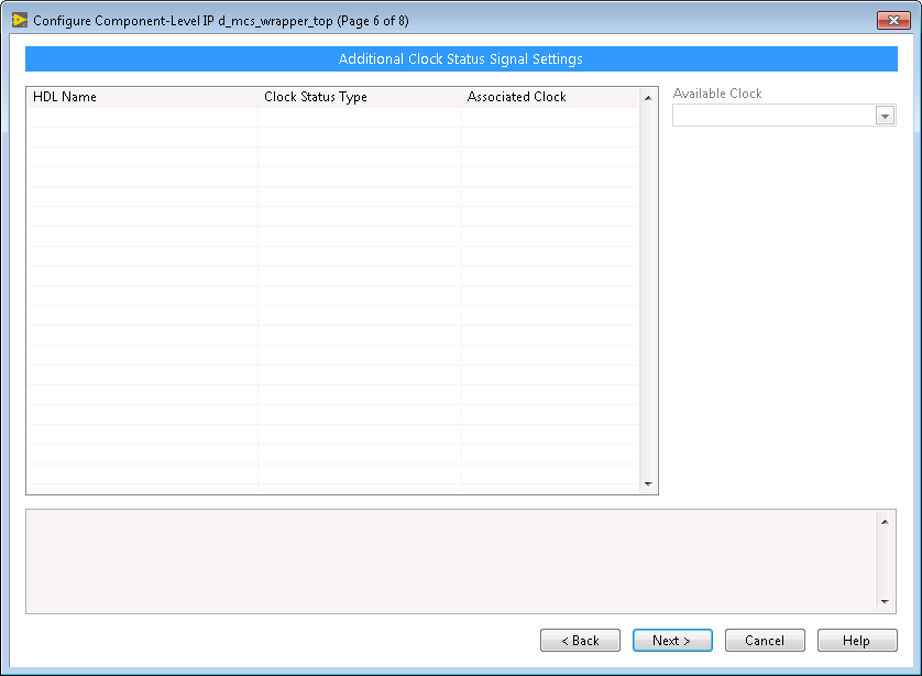
Step 26 – Nothing to do here, just click next.
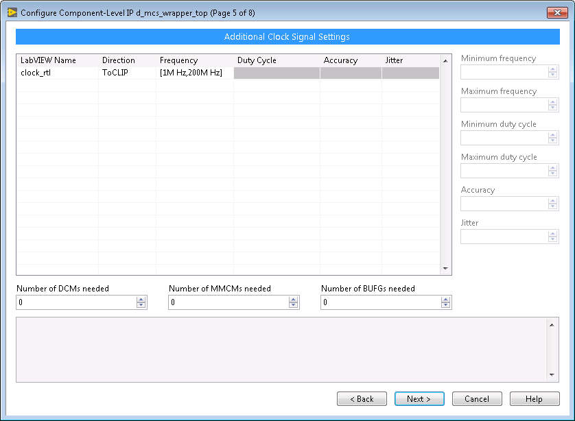
Step 27 – Nothing to do here, just click next.
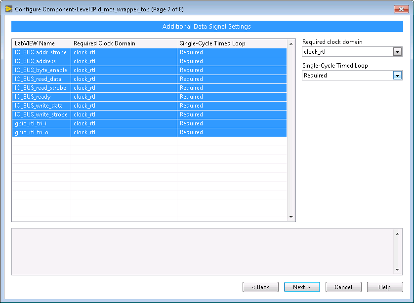
Step 28 – Use the shift key and the mouse to select all signals on the left, and make them all require the clock_rtl clock domain and to be required to be inside a Single-Cycle Timed Loop.
Step 29 – Click Finish
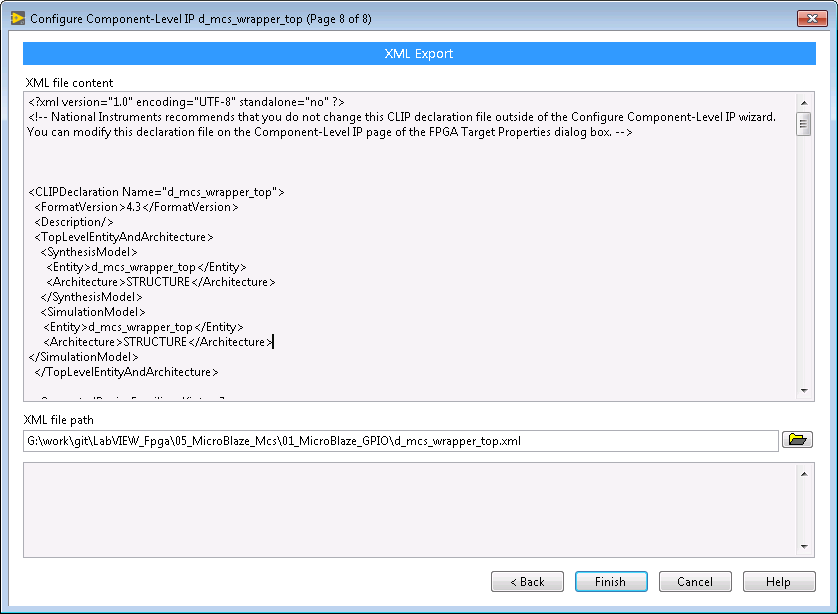
Step 30 – And now you have a CLIP available to your project.
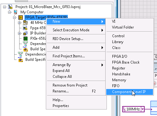
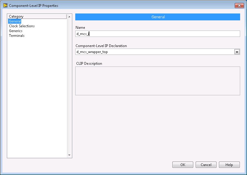
Step 31 – Now create an instance of this CLIP by clicking New->Component Level IP
Step 32 – Select the ip from the drop down, I usually name the instance to match what is in the wrapper vhdl file. In older versions of LabVIEW this was required, but I am not sure if that is still the case.
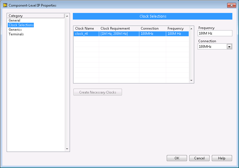
Step 33 – Select the appropriate clock
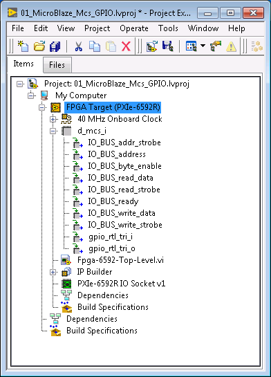
Step 34 – What the project looks like with the added CLIP after expanding it.
Step 35 – Inside the Single-Cycle Timed Loop, right-click and select an “I/O Node”
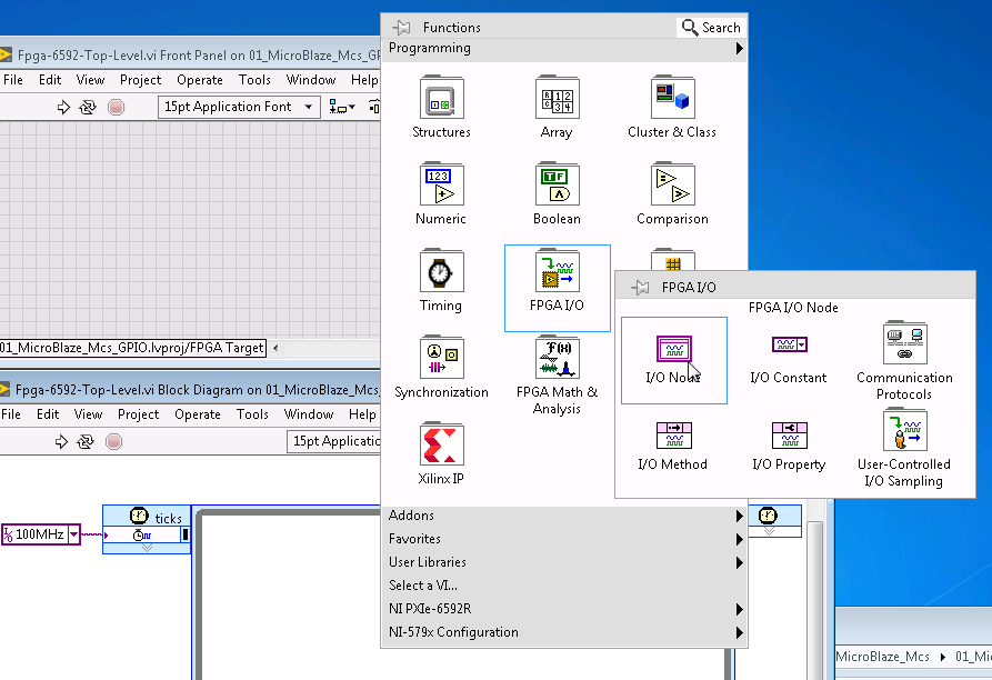
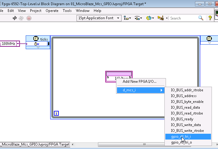
Step 36 – From here select the gpio_rtl_i, and gpio_rtl_o signals.
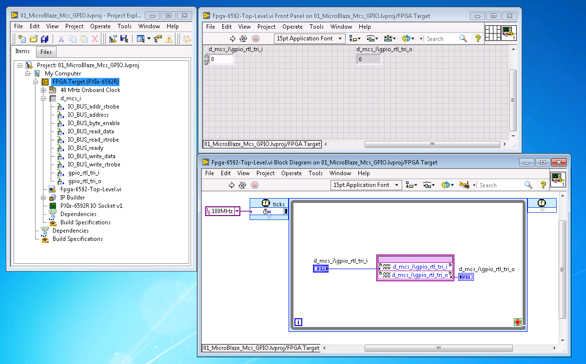
Step 37 – Add a control to the input, and an indicator to the output.
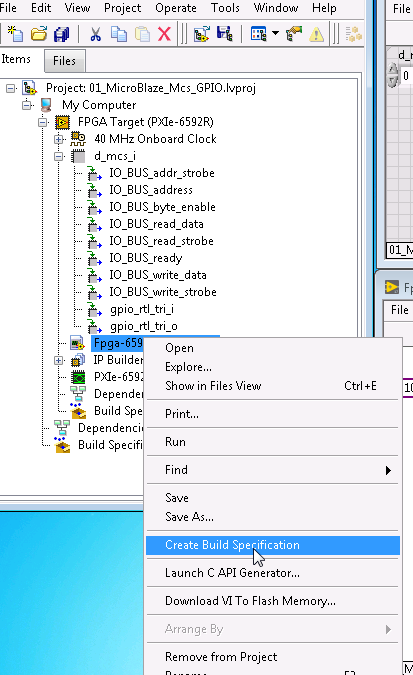
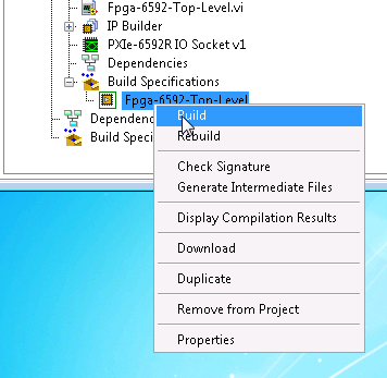
Step 38 – Create a Build Specification
Step 39 – And build it!
You can now run the top-level VI. Video demonstration to come shortly.