
Working from scratch, I created a LabVIEW FPGA project that imports a MicroBlaze design that communicates with LabVIEW via a UART, and has the ability to change the elf file in a much shorter time frame than before.
I did this by adding the MicroBlaze to the project after it had been exported to Vivado, and not from within the CLIP that is imported as before. The only bad news is that I have to synthesize the FPGA project from Vivado, which currently is not connected to the NI FPGA Compile Cloud. This may be a feature that is coming soon, but it will only come if users start using this the Project Export to Vivado feature in the first place. So please write me any comments if anything is confusing or hard to follow below!
YouTube Video Demonstration
Source Code
See my github repository here:
https://github.com/JohnStratoudakis/MicroBlaze_UART
Part 1 – Create and Export a MicroBlaze Design
We are creating a MicroBlaze design, settings all of our processor options, including adding an instance of the UARTlite IP core, and exporting this Block Design to a tcl script that we will later on import in to our LabVIEW FPGA generated Vivado Project. We will not export the hardware or create any elf files in this part.
- Create a new project from within Vivado 2015.4 (this is important, it will likely not work from other versions of Vivado)
-
- The first step is not that important, you can just click next
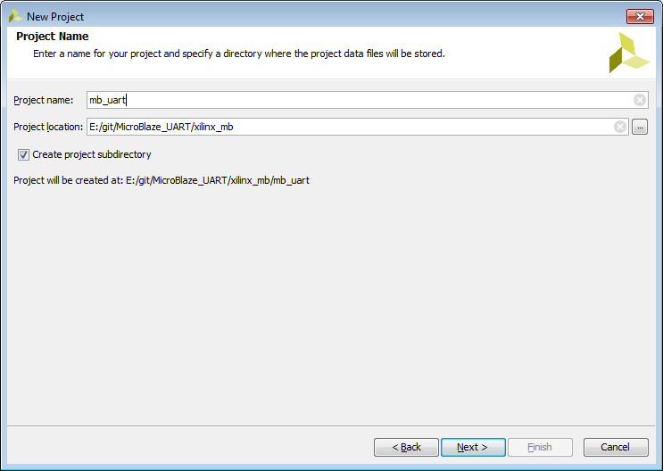
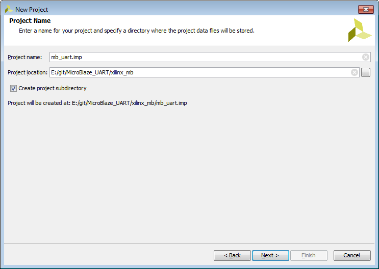
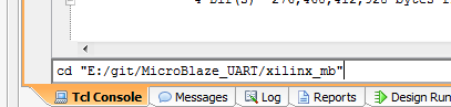
- I selected the project location to be on my E drive, “E:/git/MicroBlaze_UART/xilinx_mb”, and the name of the project to be “mb_uart”.
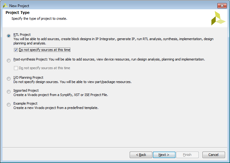
- This is an RTL project type, and we do not want to specify any sources at this time.
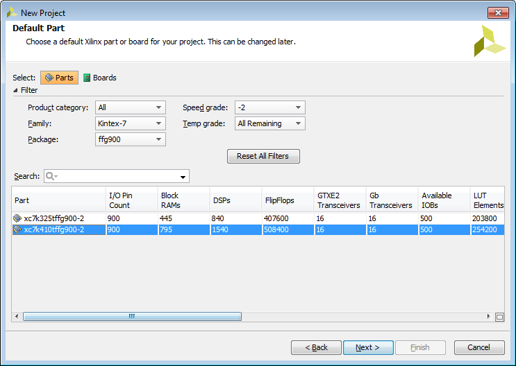
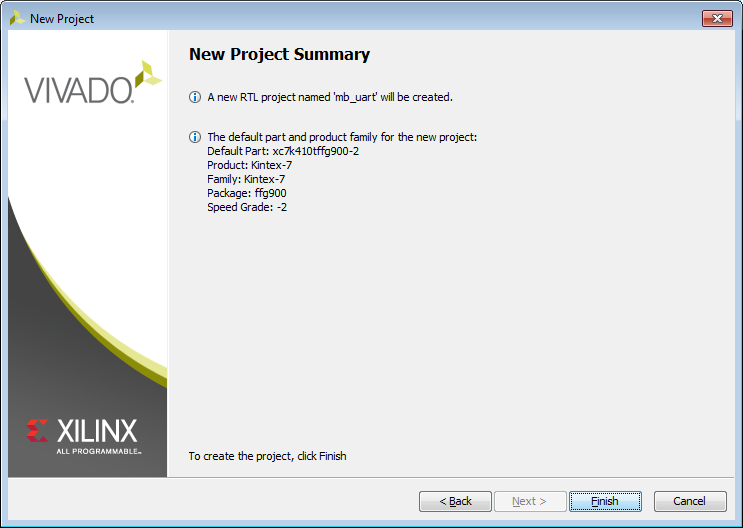
- The PXIe-6592R board contains a Kintex-7 FPGA chip with the following parameters:
- Part #: xc7k410tffg900-2
- Family: Kintex-7
- Package: ffg900
- Speed Grade: -2
- New Project Summary, just click finish
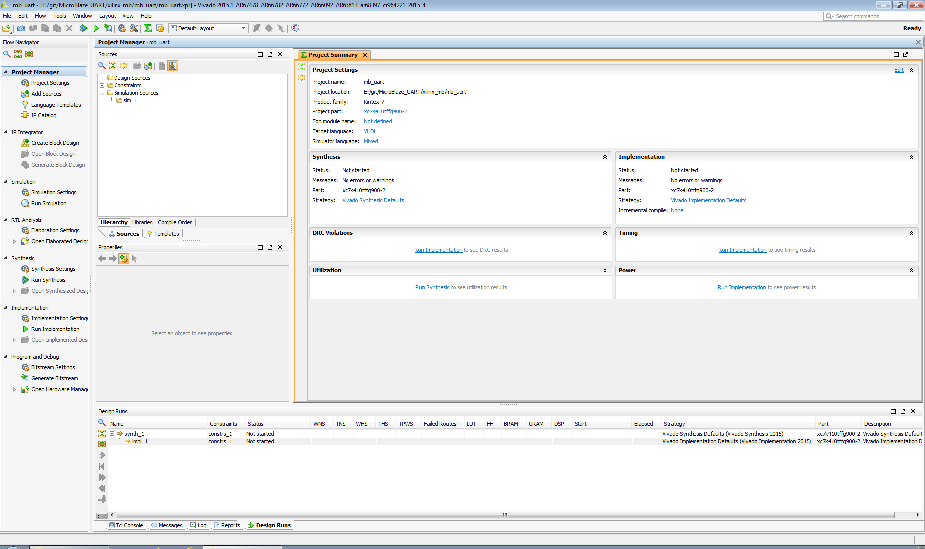
- What an empty project looks like:
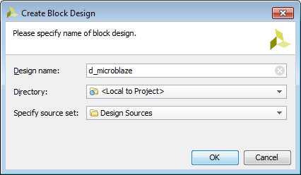
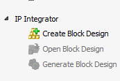
- Now create a block design
- I have been going with the “d_” d underscore followed by microblaze naming schema
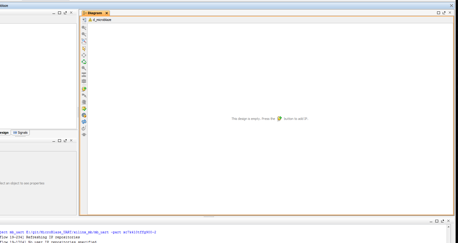
- Now look at the empy Block Design
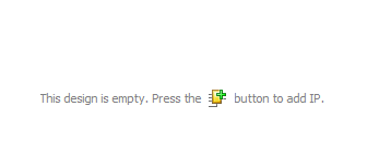
- Click on the “Add IP” button
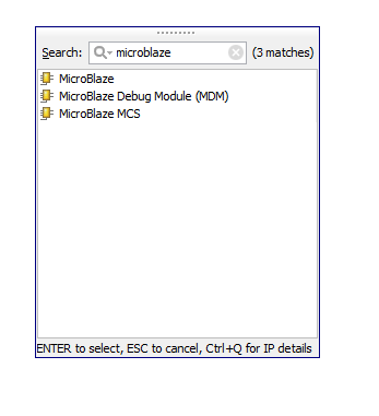
- Start typing in MicroBlaze, and make sure you select “MicroBlaze” and not “MicroBlaze MCS”. The MicroBlaze MCS is a striped down version of the MicroBlaze which is very easy to use, but hard to bring in to LabVIEW. Well, it is not hard to bring in to LabVIEW, I just have not figured out how to bring it in and for the UART to work!
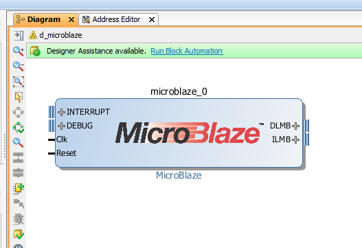
- Look at the MicroBlaze IP. I hear in older version of the Xilinx Tools – namely ISE – there was no such picture, but instead you were given a list of signals and ports…
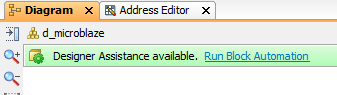
- Now click on “Run Block Automation”, this will bring up a wizard where you can set a bunch of parameters, such as how much memory should be used and what peripherals it can support
- This is what the defaults look like:
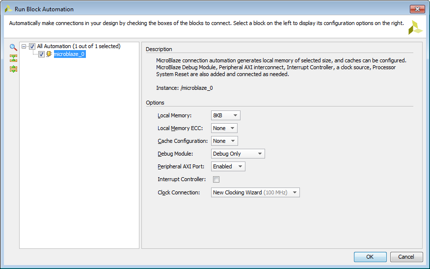
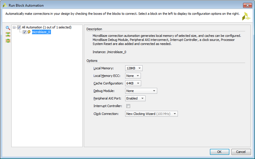
- I set the following parameters:
- Local Memory: 128KB
- Cache Configuration: 64KB
- Debug Module: None (Can’t debug from LabVIEW at the moment)
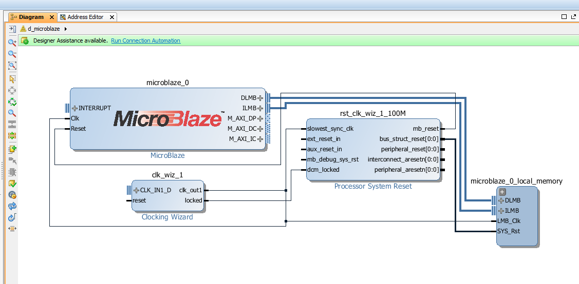
- Here is what it looks like after block automation. Notice the local memory block, the Processor System Reset icon and the Clocking Wizard
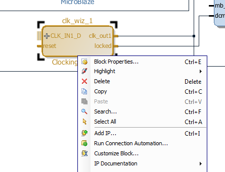
- I want to remove the reset from the Clocking Wizard and to convert the input clock to a single-ended clock from a differential clock. A differential clock just means that there are 2 clock signals and they always have to be opposites of each other.
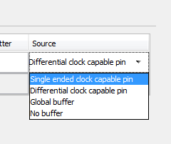
- Here I switch the clock from “Differential Clock” to “Single-Ended Clock
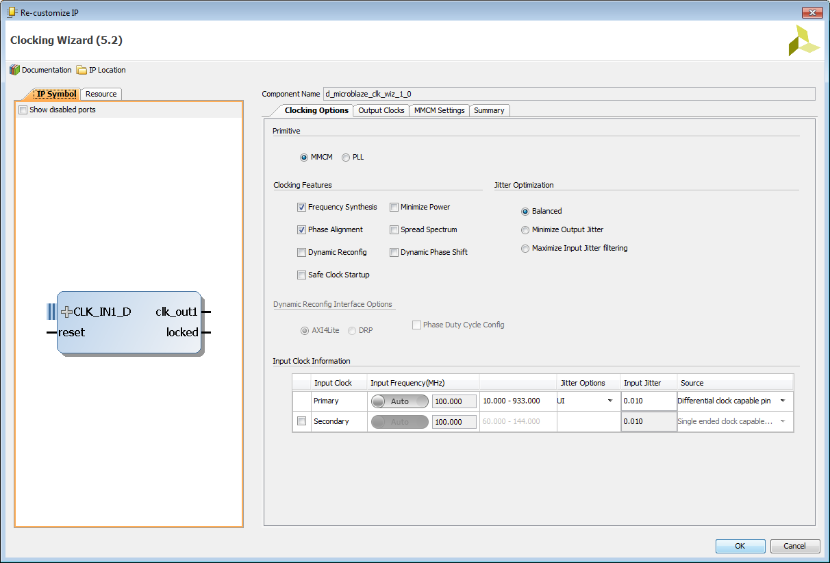
- Here I get rid of the Reset signal, notice how the Reset Type gets grayed out automatically.
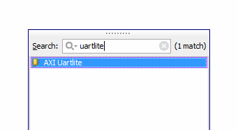
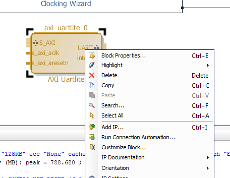
- Now I add the “AXI Uartlite” IP. There is another UART IP that is available, but I have arbitrarily chosen to learn by using this one.
- Now I want to customize the Uartlite IP, so just as before with the Clocking Wizard, I right-click (away from any terminals) and select “Customize Block”.
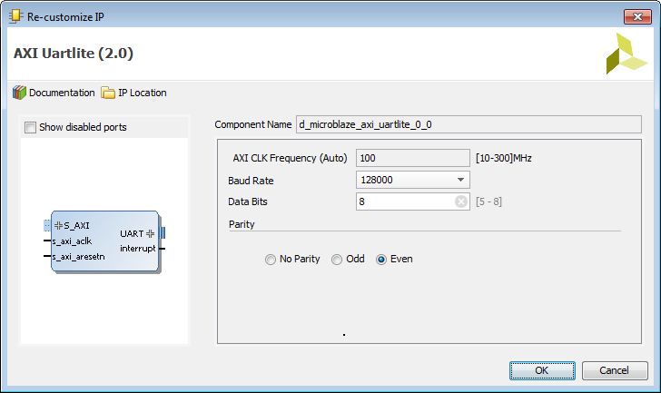
- I set the Baud Rate to 128,000, I leave the number of data bits to 8, and I set even parity. Note that I chose to add a parity because I want my UART connection to be more exact and to receive less (if no) garbled text.
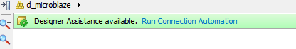
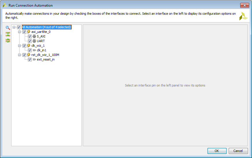
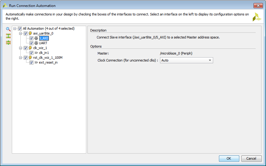
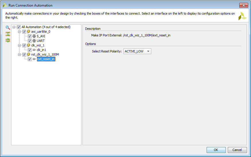
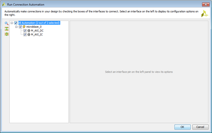
- Now for the fun part… Click on “Run Connection Automation” and watch as Vivado wires up all of our IP and components together!
- All of the default options are fine, but I have included screen shots so that you can see all the details yourself:
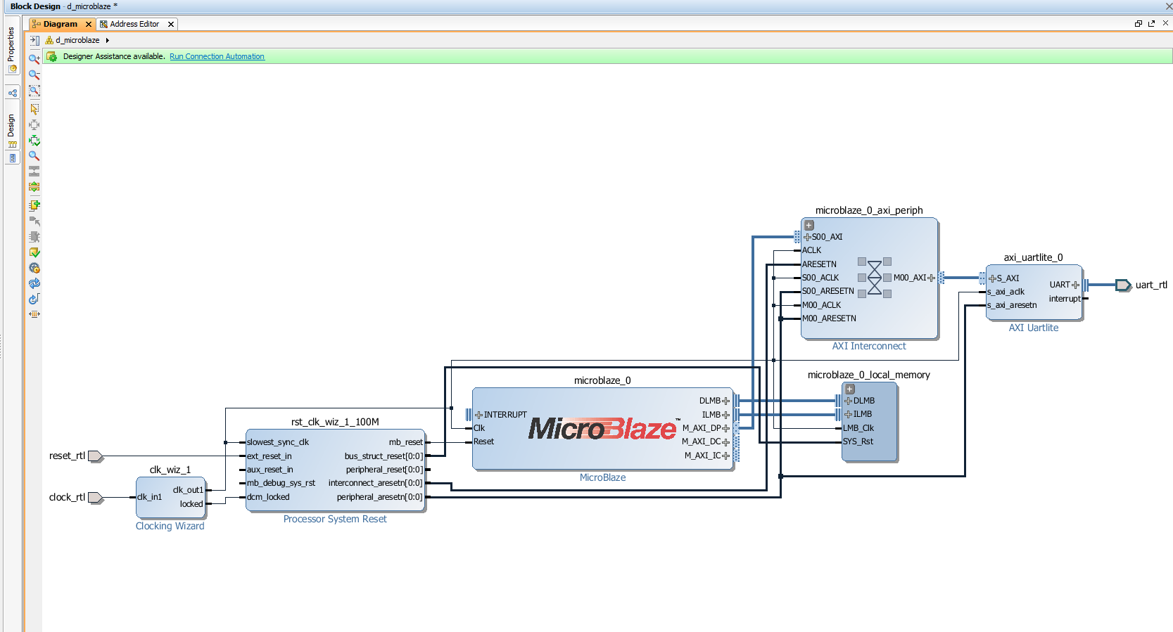
- Now after this completes, the block design will look pretty messy, so click on the “Refresh” looking icon below to regenerate the layout:
- Here is a cleaned up version of the Block Design. Notice that the “Run Block Automation” option is still there. Nothing has gone wrong, this text is there because we now have to wire up the Data and Instruction Caches.
- Again, the default options are fine
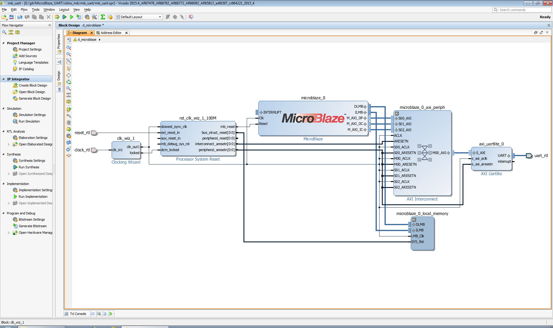
- And finally… our block design is ready.
- Now we will generate an HDL Wrapper file. This is not required for the Block Design, but it will help us with the importing of this design in to LabVIEW later.
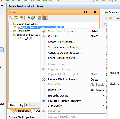
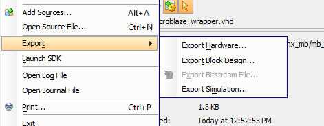
- Now we will click on “Export->Export Block Design”, this will generate a tcl script that we can run or “source” from another Vivado project and this block design will be regenerated for us.
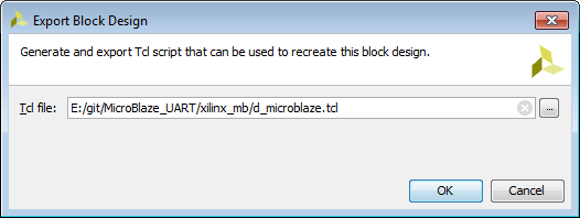
- Note the location of the wrapper VHDL. Copy this file to your clipboard
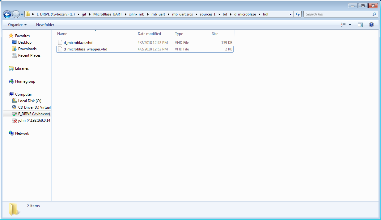
- Place it in to the root directory of your project, a location that you will commit to source control.
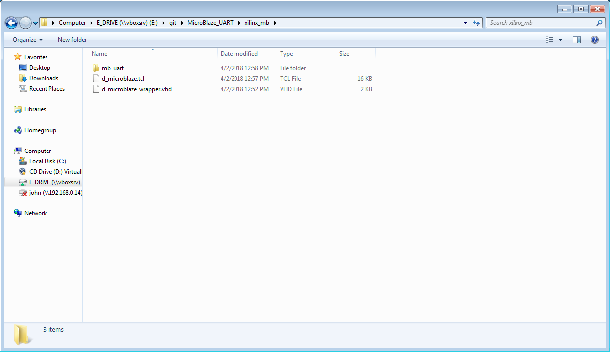
- The Tcl file should also be in the same directory
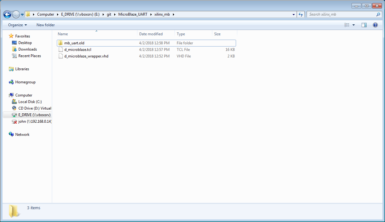
Part 2 – (Optional) How to Recreate MicroBlaze Design from Source TCL Script
So Vivado is not like other programming languages where you create your gitignore file and commit the rest to source code control. In Vivado, you generate a TCL script that will re-generate your entire project – or in our case – a specific Block Design. This script will also import any other files such as VHDL files or constraints files that are required. In our case we have a very simple design that does not require any such helper files.
- Click on Create New Project:
- Same as before, first couple of steps just click “Next”

- This time I will call the project “mb_uart.imp”, to differentiate it from the project that I created.
- Again, RTL project, and do not specify any sources at this time

- Same part as before. Not sure if you can import a block design to other FPGAs, perhaps if they have the same family or series, but I have not tried this out yet.

- Project Summary

- Click on “Tcl Console”
- Change to the directory where the Tcl export script is located
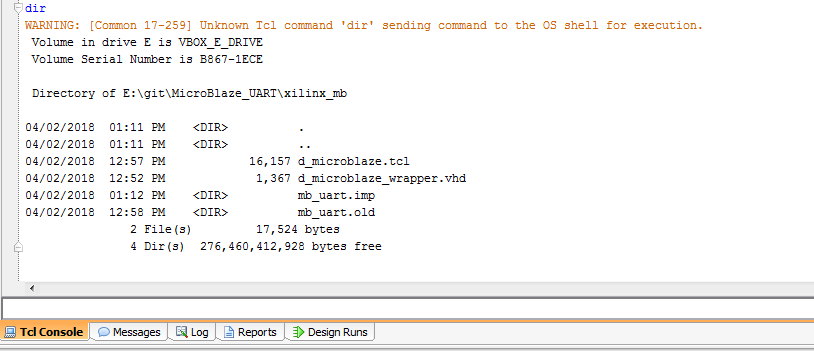
- Type dir if you like. Notice how “known Tcl” commands are sent to the underlying os for execution
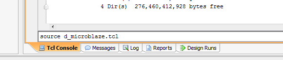
- And finally, “source” the tcl script
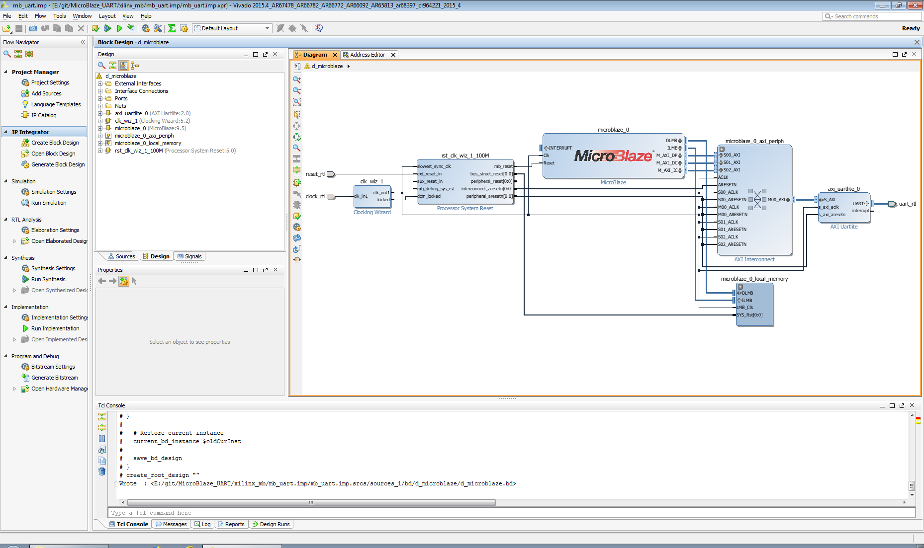
- And here is the imported Block Design
- And that’s it! Create an HDL Wrapper if you like
Part 3 – Bring Design in to LabVIEW FPGA
Now we have to create a CLIP (Component Level IP) Node in LabVIEW FPGA that will import this MicroBlaze Block Design. A CLIP node contains a top-level vhdl wrapper that usually instantiates the IP that we want to bring in to LabVIEW FPGA, but in this case I am creating a CLIP node that contains an empty wrapper for the MicroBlaze Block Design.
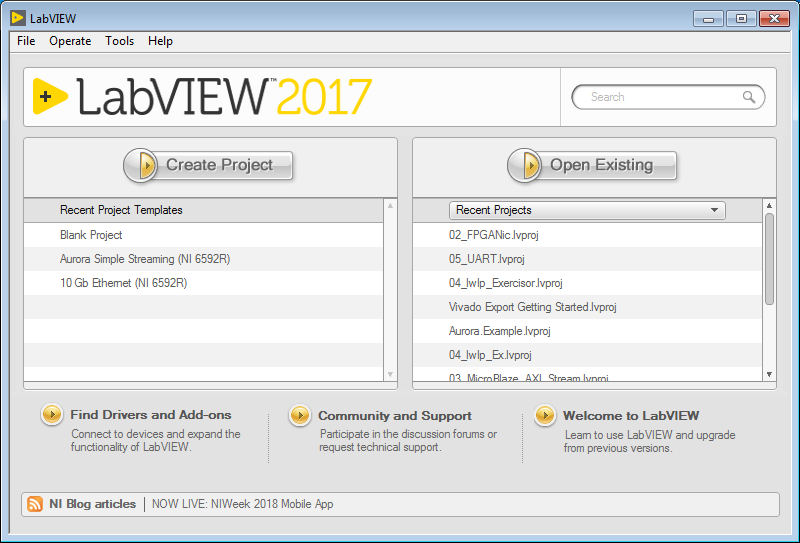
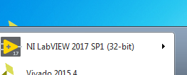
- Launch LabVIEW 2017 (32-bit) from the start menu
- Here is the screen that appears after you start LabVIEW
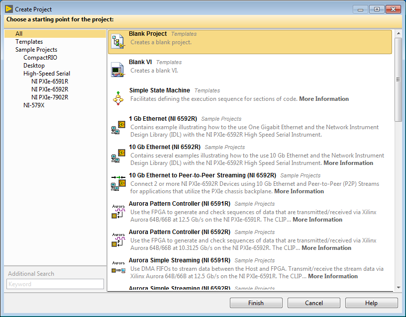
- Click on “Create Project”, Blank Project should be fine.
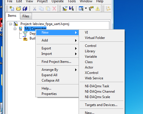
- Right-click on the “My Computer” icon and select “New->Targets and Devices…”
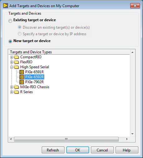
- Select “New target or device” and select the PXIe-6592R FPGA board
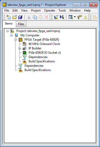
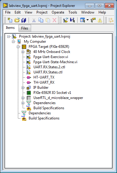
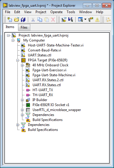
- Here is what the project looks like after adding the FPGA device/target:
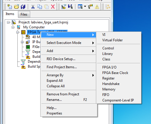
- Create a FIFO for communicating from the Host to the FPGA Target, aka “Host to Target – DMA” by clicking New->FIFO:
- I follow a naming standard that ALE System Integration follows which is to prepend “HT” or “TH” to the name of each FIFO, where HT stands for Host to Target, and TH stands for Target to Host, so I name this FIFO “HT-UART_TX”:
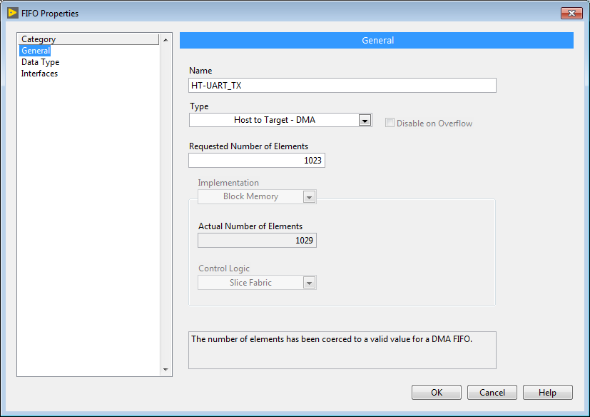
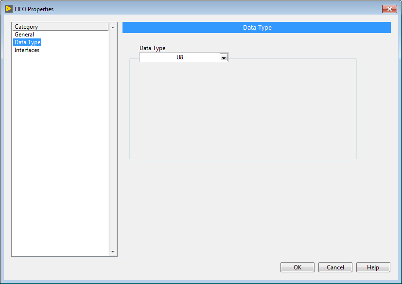
- I also set the Data Type of this FIFO to U8, because it will be used to receive characters
- The same thing for the Receive FIFO, “TH” for Target to Host, and RX for Receive.
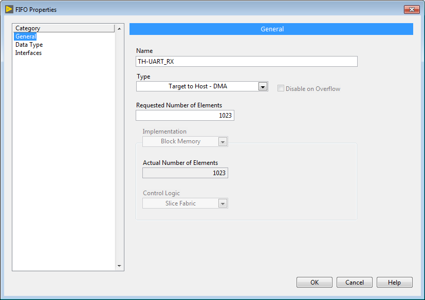
- Data type, again is U8.

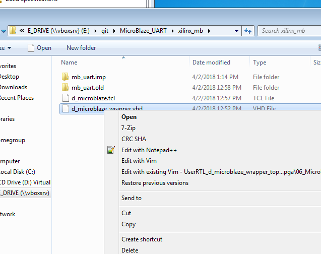
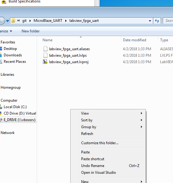
- Now do you remember where the microblaze wrapper vhdl was located? Find it and copy it to the root of the LabVIEW project
- The LabVIEW project is located in the MicroBlaze_UART/labview_fpga_uart directory:
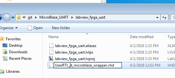
- Rename the file by prepending “UserRTL_” to the name of the file.
- Edit the file, here is what it looks like before: (Sorry for the screen shot, I will provide source code links soon):
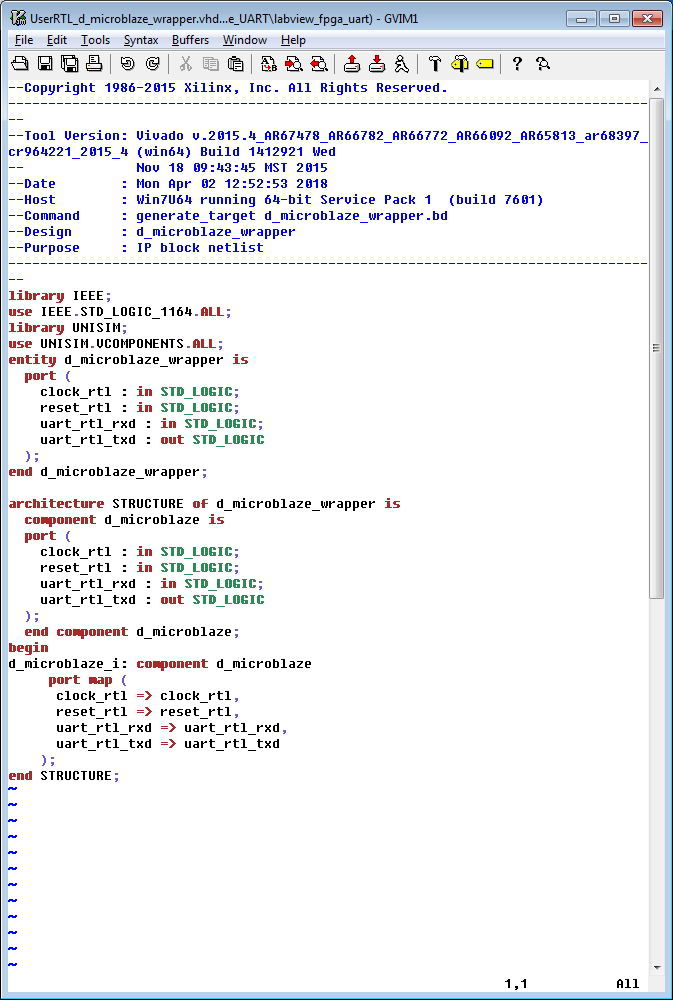
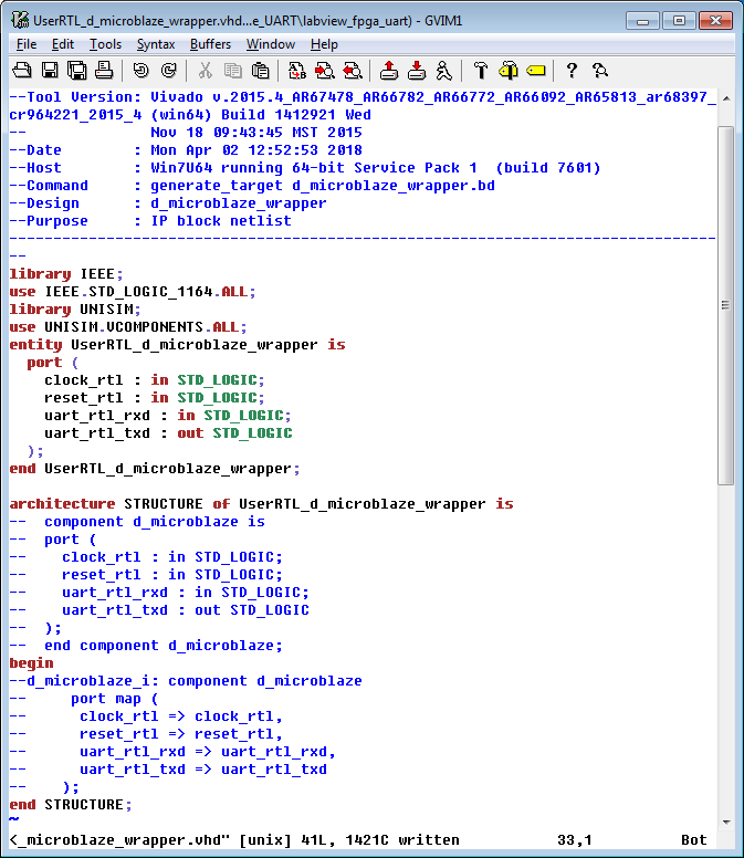
- Change the name of the entity to match the file right now
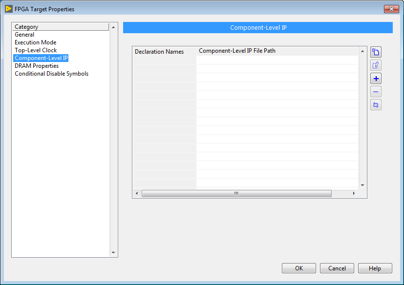
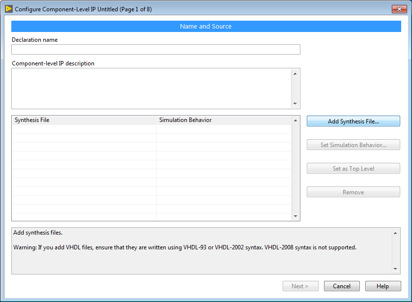
- Now we will create a CLIP, right-click on the FPGA target and select “Properties”
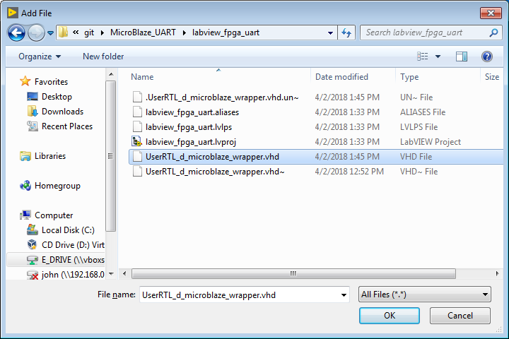
- Add the VHDL file that we edited before – “UserRTL_d_microblaze_wrapper.vhd”
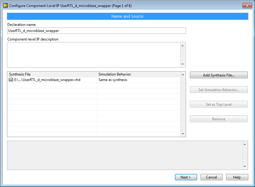
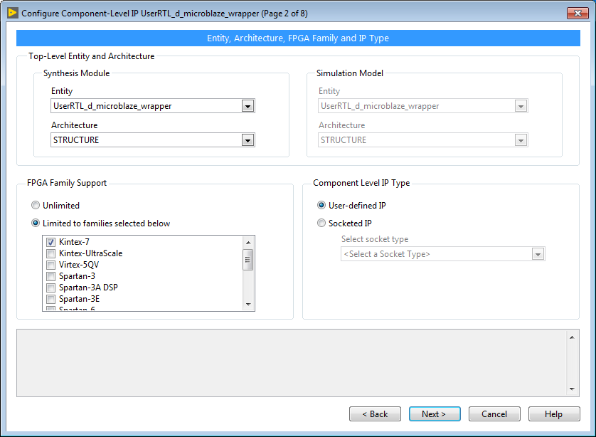
- Then click Next to go to step 2 of 8. Here select the “Limited to families selected below” option:
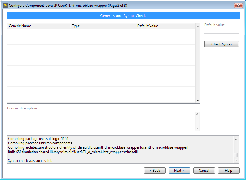
- Then click next to go to step 3, here you have to click on “Check Syntax” and a Xilinx application is run to check the syntax
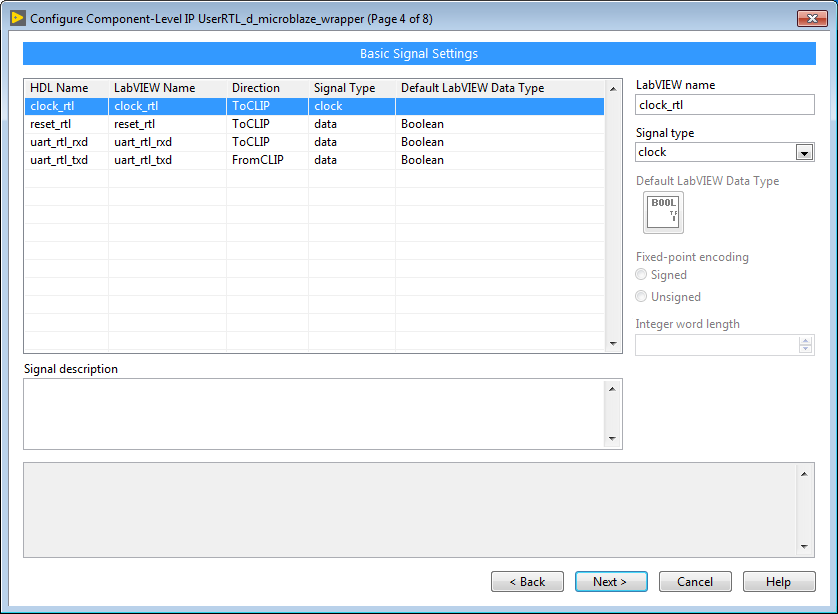
- Now for step 4, click on the “clock_rtl” signal and make sure it is set to “Signal type” of clock. Don’t worry about the reset signal, we want to control this ourselves.
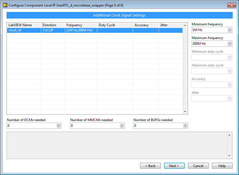
- For step 5, nothing is required, so skip and go to step 6
- Same thing for Step 6, just click next
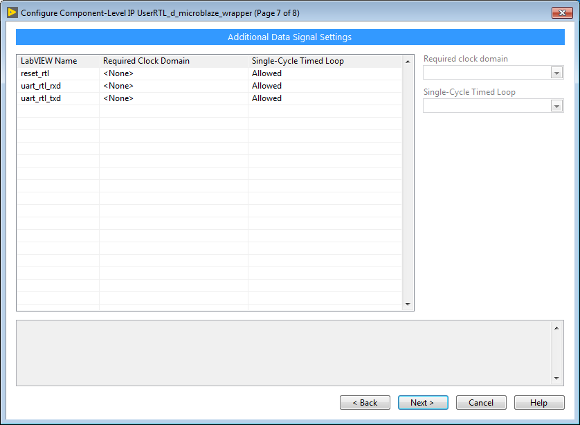
- For step 7, just make sure that all signals are “Allowed” inside a Single-Cycle Timed Loop. You can probably also required this, but we will not be doing that today.
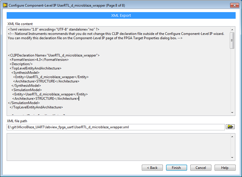
- Step 8 – Click Finish.
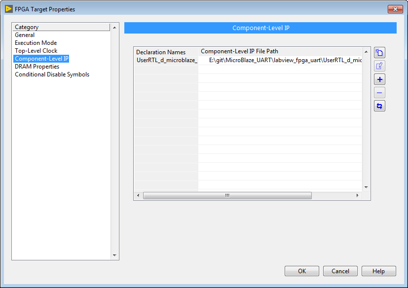
- We are finished, now a CLIP is available for us to use in our FPGA design, but it has not been instantiated. I believe you can have multiple instances of the same CLIP.
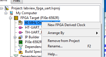
- Before we go any further, we have to add a clock for the MicroBlaze. Our design will be 100 MHz, so right-clock on the 40 MHz clock and click on “New FPGA Derived Clock”
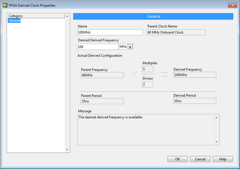
- Type 100 in to the “Desired Derived Frequency” box, and everything else should automatically update. Then click OK
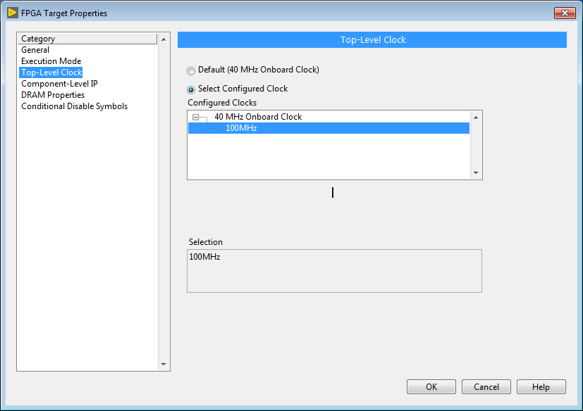
- Now we also have to set our top-level clock to be 100MHz. So right-click on the FPGA Target and select properties, and in the following dialog select “Top-Level Clock” and select the new clock.
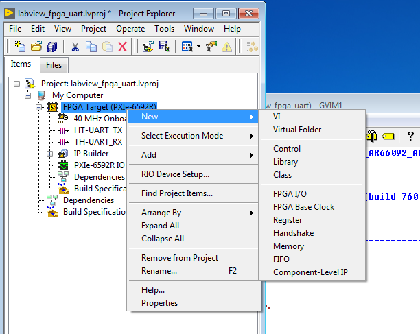
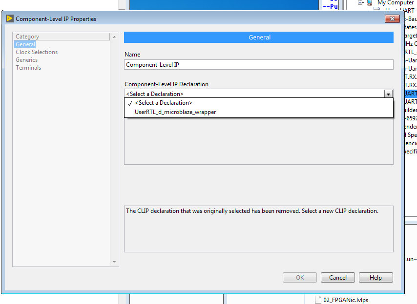
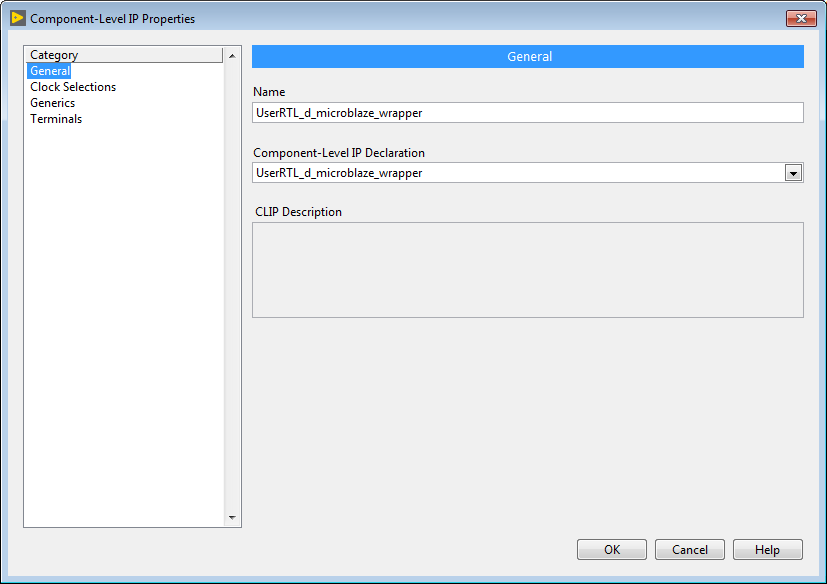
- Now we will add an instance of the CLIP. Right-click on the FPGA Target and select “New->Component-Level IP
- Select the UserRTL_d_microblaze_wrapper
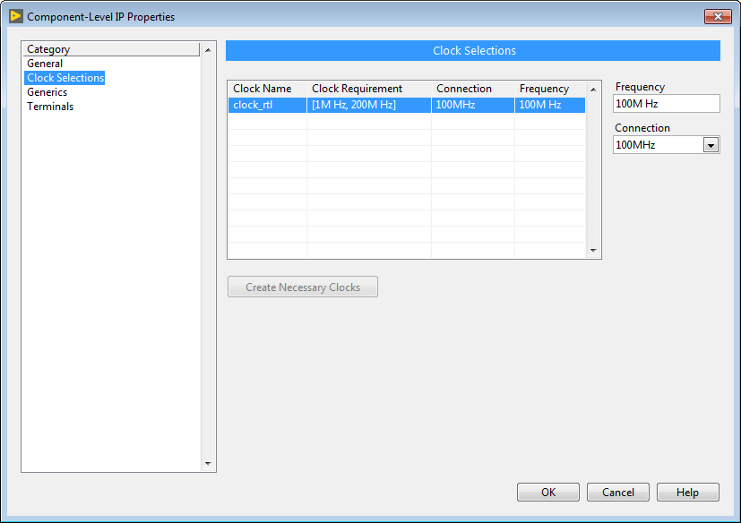
- And on the “Clock Selection” page, select the 100MHz clock.
- Now we will add some existing vi’s
- And here is what our final project looks like:
Part 4 – Create LabVIEW Host Wrapper
LabVIEW Host applications run as native Windows processes
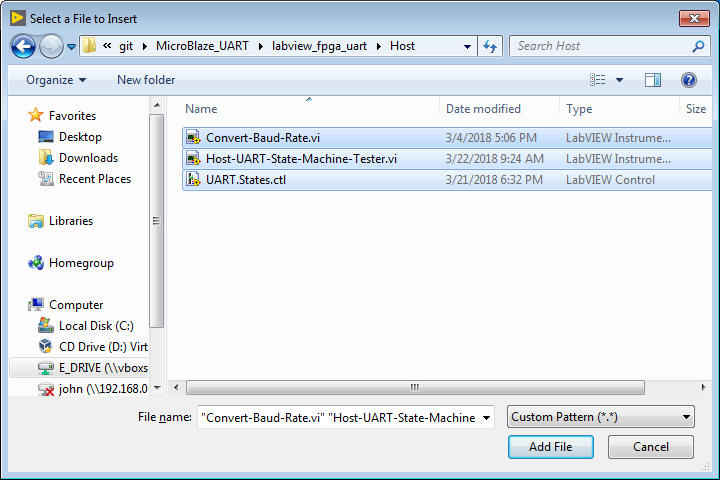
- Now we will add the Host LabVIEW application vis. A LabVIEW Host application is a native Windows executable and thanks to a bunch of libraries written by National Instruments will handle all of our communications with the FPGA.
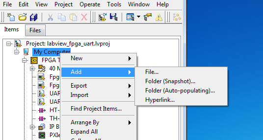
- Add the existing files
- Here is what the project looks like with all of the Host VIs.
Part 5 – Export Project to Vivado
LabVIEW has introduced a new feature, the ability to export an entire FPGA design to Vivado, which allows you to import any existing IP. All you have to do is define one or more CLIP IPs that define the interface with your design.
- Right click on the Build Specification inside the FPGA Target and select “New->Project Export for Vivado”
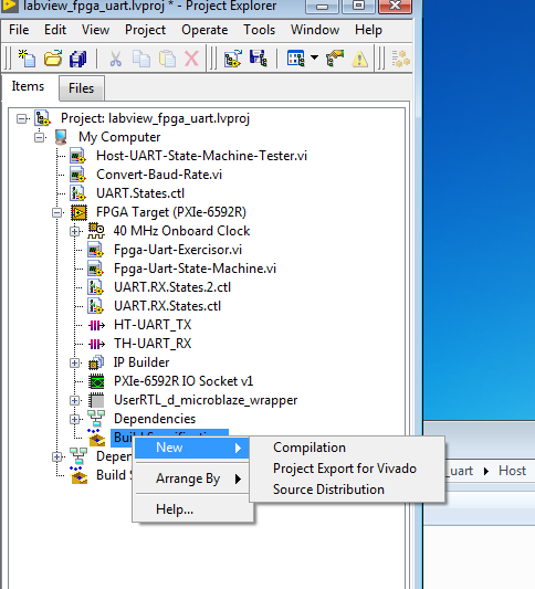
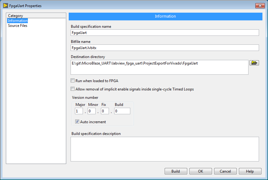
- Give the build specification a name, I recommend keeping it short and sweet. So change it from “My Project Export for Vivado Design Suite” to something like “FpgaUart”
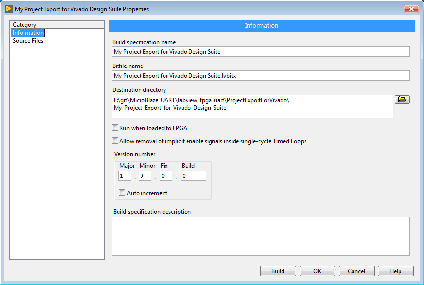
- I always set “Auto increment” to true.
- Then on the “Source Files” tab and select the “Fpga-Uart-Exercisor.vi” to be the top level
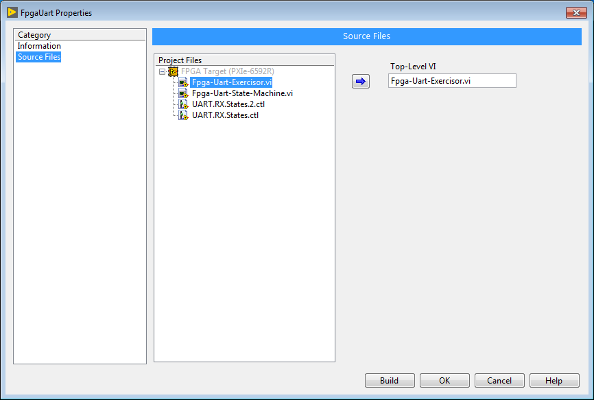
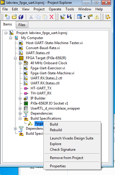
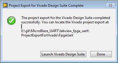
- Now there is a new Build Specification. Clock on Build
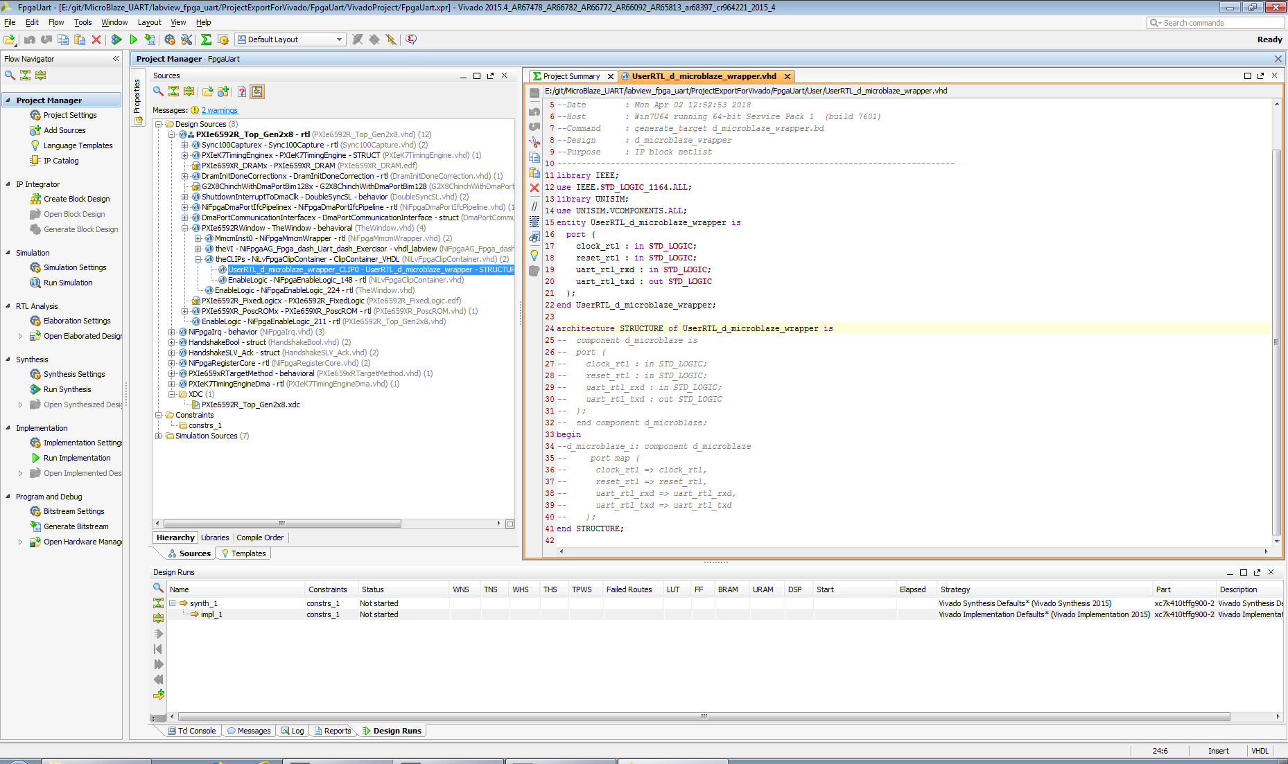
- After it completes, you can launch Vivado by clicking on the button below.
- Here is what the Vivado project looks like. All of the IP files are encrypted, except for the files we added for our CLIP. Since we added only one file, that is all we will see.
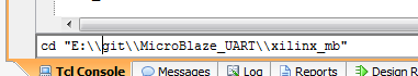
- Now we will import our Block Design. Locate the “Tcl Console” in the bottom window.
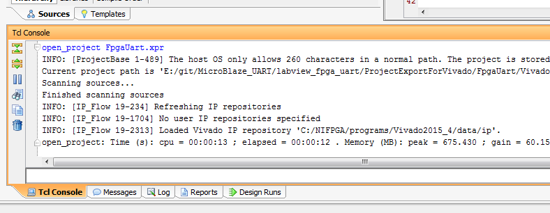
- This console supports TCL commands as well as regular operating system commands. Since we are on Windows, we would like to change our current working directory to be where our d_microblaze.tcl file is located. Remember, Vivado uses the backslash ‘\’ as its escape character, so you will have to enter the backslash twice for each time you would like to use it.
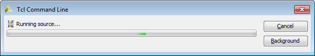
- Now we have to source our file by issuing the “source d_microblaze.tcl” command:
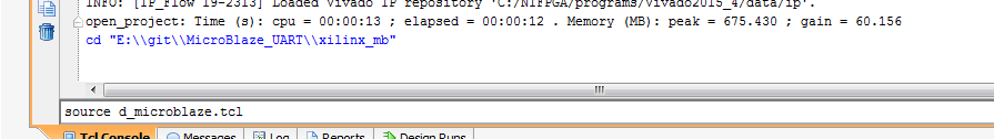
- This will take a couple of seconds, depending on the speed of your computer.
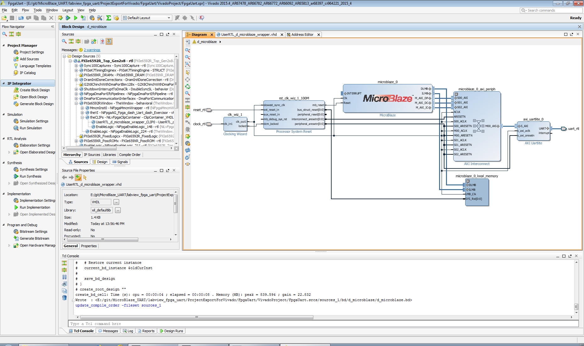
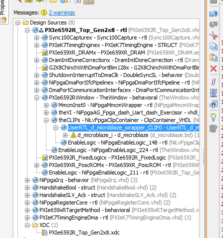
- After it finishes importing/re-creating the design, this is what you should see:
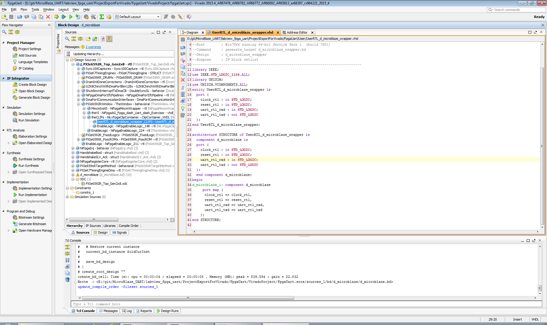
- Now we go back to our “UserRTL_d_microblaze_wrapper.vhd” vhdl wrapper file and remove the comments enabling the code that uses the MicroBlaze.
- Now you will see that this new design appears under the VHDL wrapper file
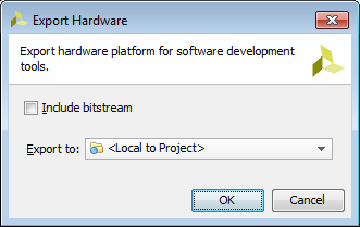
- Now we have to export this entire design to Xilinx SDK so we can generate an executable to run. Click “File->Export->Export Hardware”
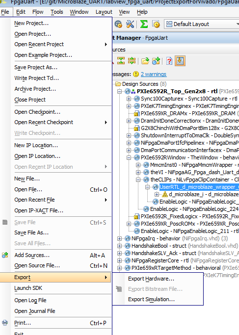
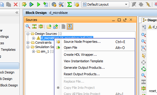
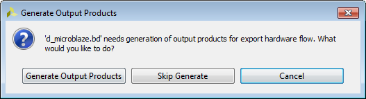
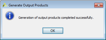
- We have not run “Generate Output Products” for the MicroBlaze, so we will be prompted to do so. Make sure you click “Generate Output Products”. If you are more experienced than me in Vivado, perhaps you know if this step is required.
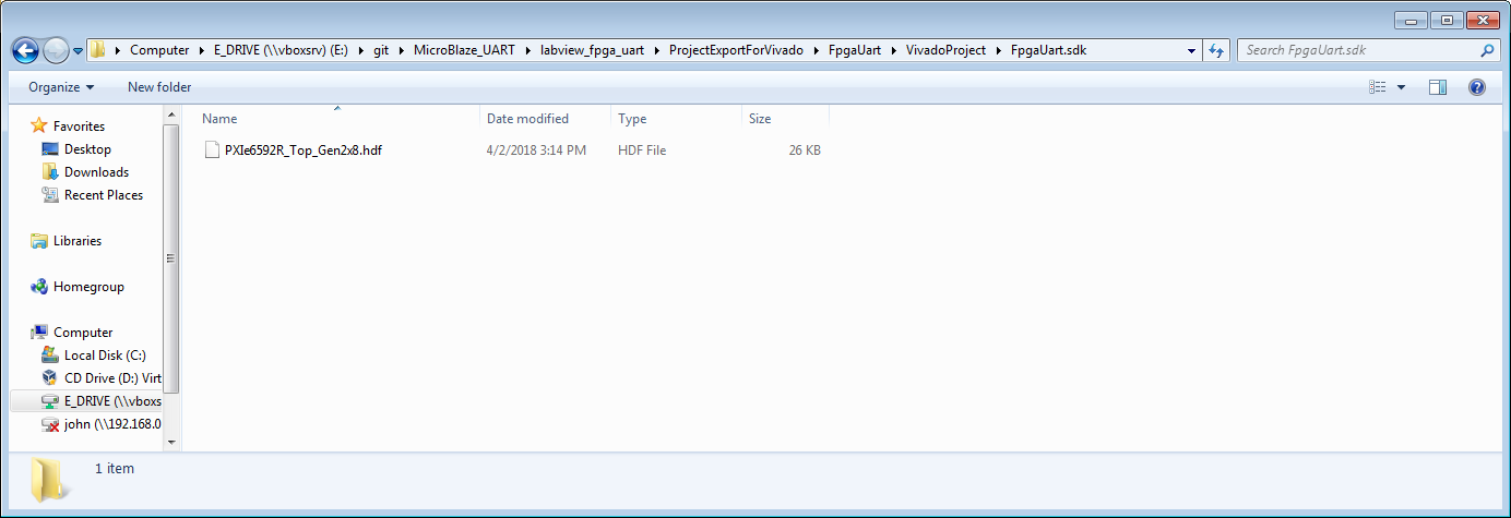
- The default directory is fine.
- The directory will be named “FpgaUart.sdk”
Part 6 – Building a C Executable for Running on the MicroBlaze Soft-Core Processor
Run the executable by referencing the lvbitx file
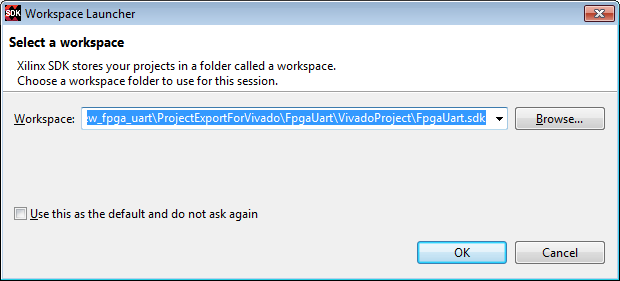
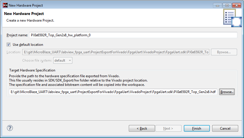
- Now open Xilinx SDK and select the “FpgaUart.sdk” directory as the workspace
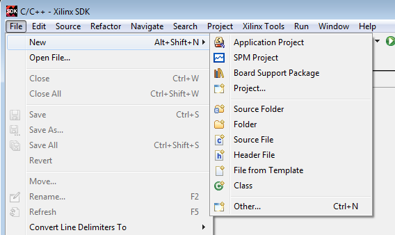
- Create a new “Hardware Platform Specification” project by clicking on “File->New->Other”
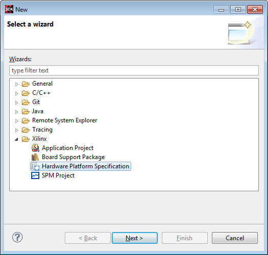
- Select “Xilinx->Hardware Platform Specification”
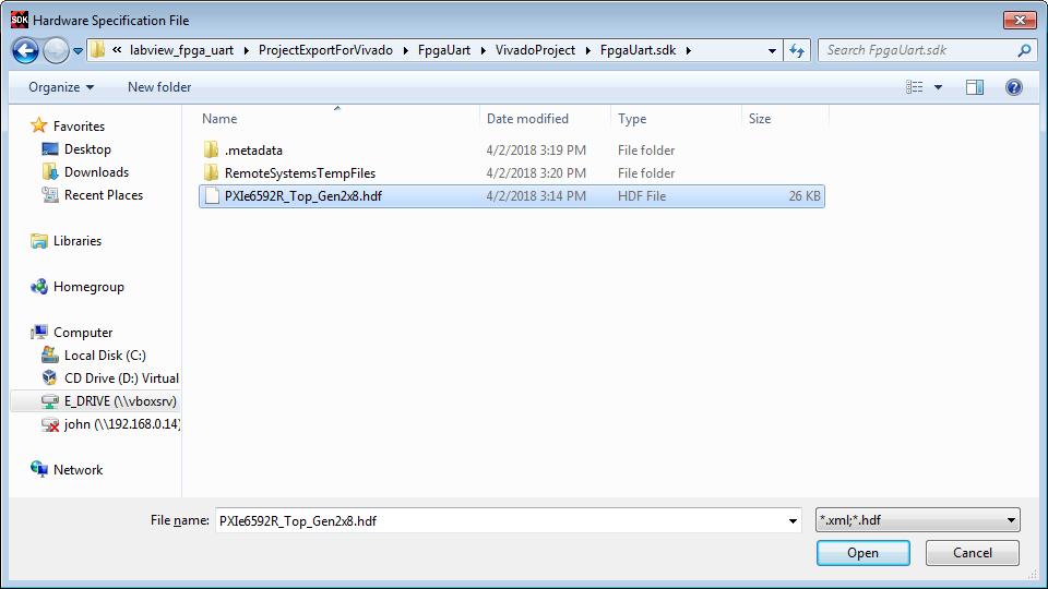
- Select the only file in the sdk directory, the .hdf file.
- The Project name will be automatically populated
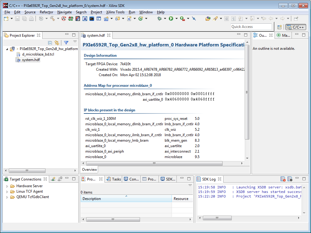
- Here is what everything looks like after creating the Hardware Platform Specification
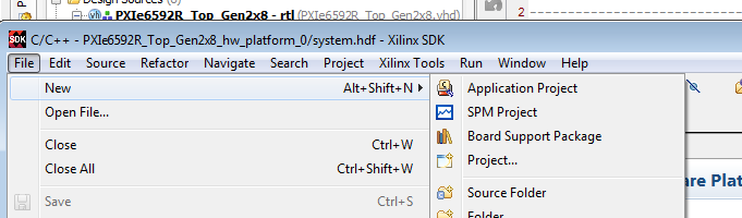
- Now create an Application Project by selecting “File->Application Project”
- Name the project “mb_uart_1” and click next.
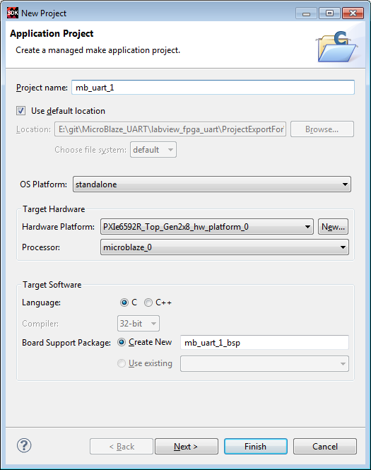
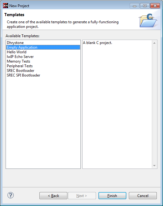
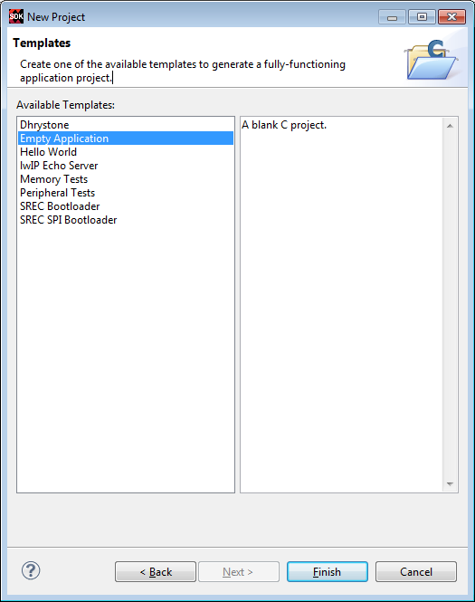
- Select “Empty Application”
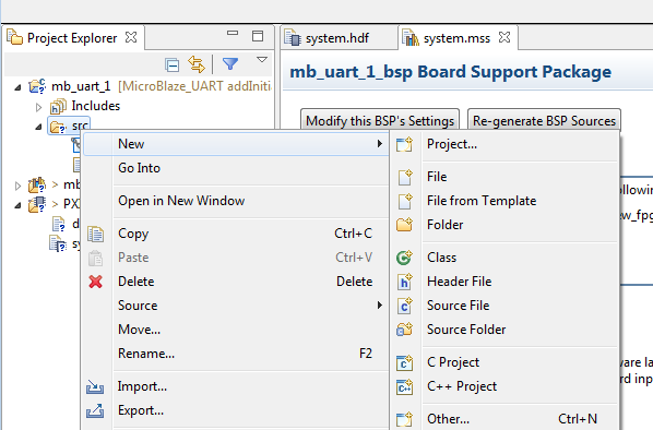
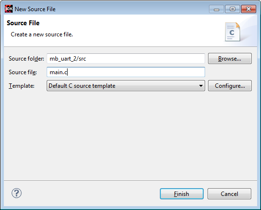
- Now we will add a new source file
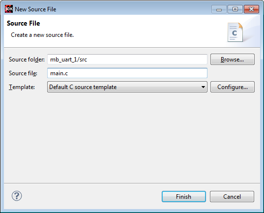
- We will call it main.c
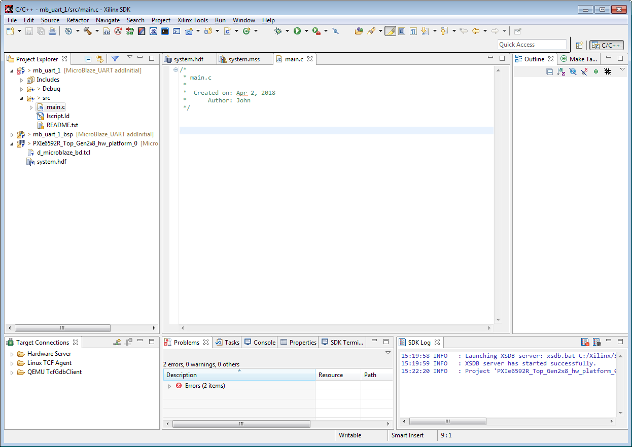
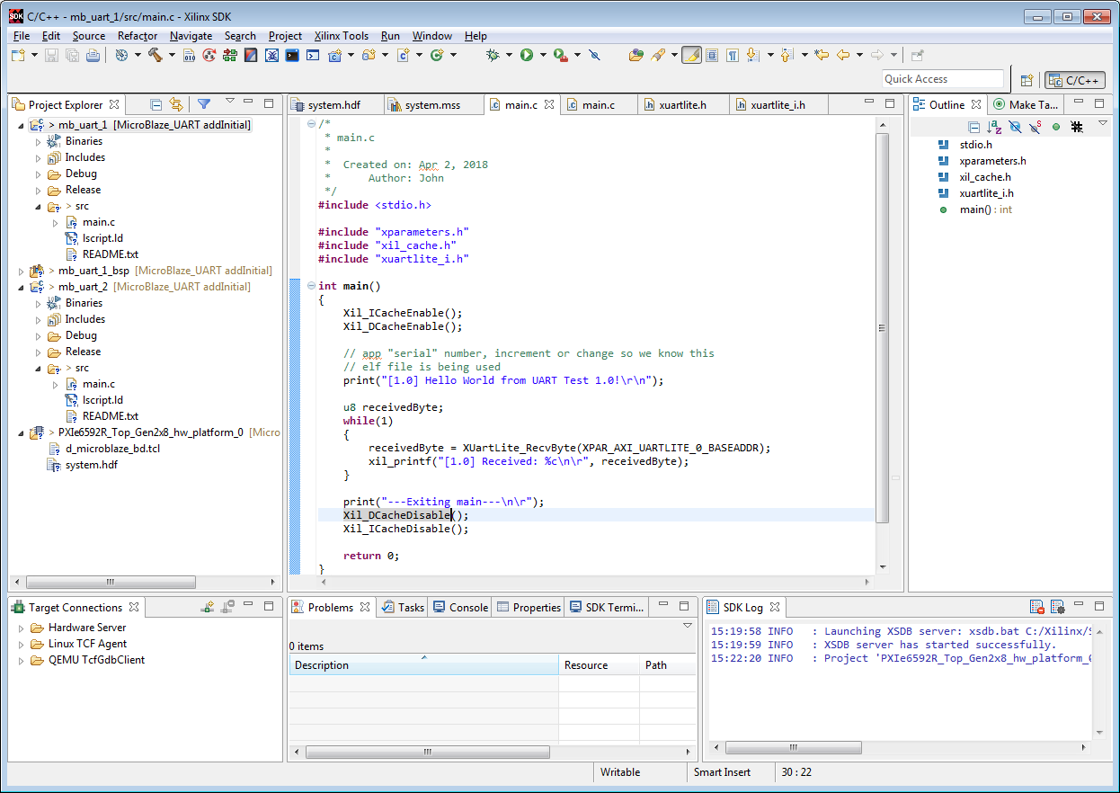
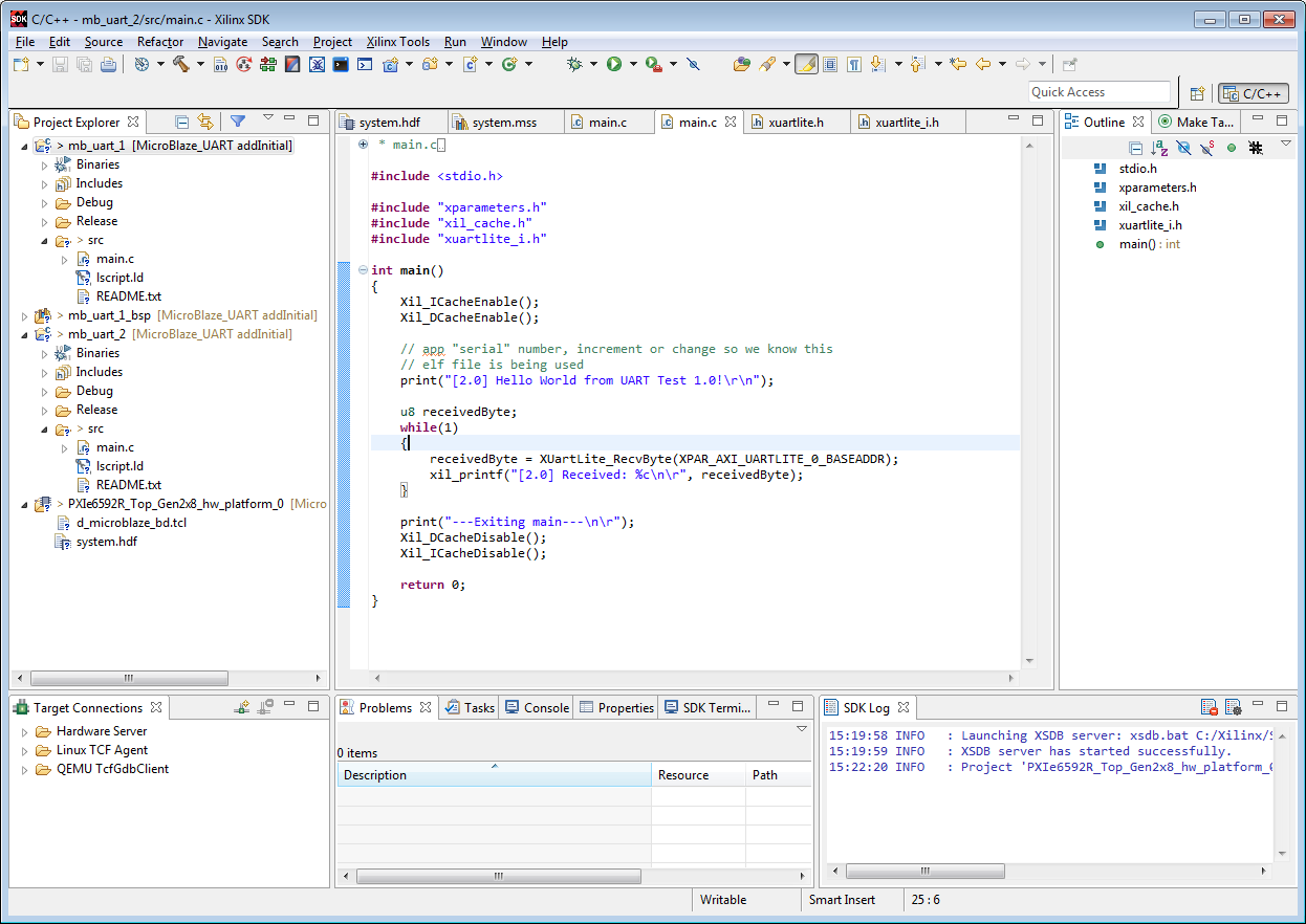
- Here is the application with an empty main.c file. Note that there are errors listed in the bottom window because this cannot build without a main function!
- After I cut and paste the source code for a simple UART application, the errors go away.
- Now I am creating a second project with the same name but with the number 2 instead.
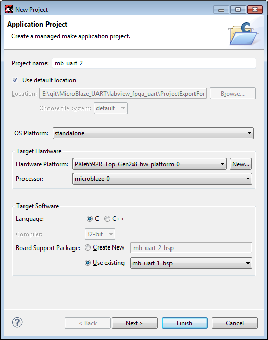
- I am going to use the same Board Support Package of “BSP” file as before, and I am creating another Empty Application.
- I add a new main.c as before.
- I paste the same source code, but this time I replace all instances of “1.0” with “2.0”
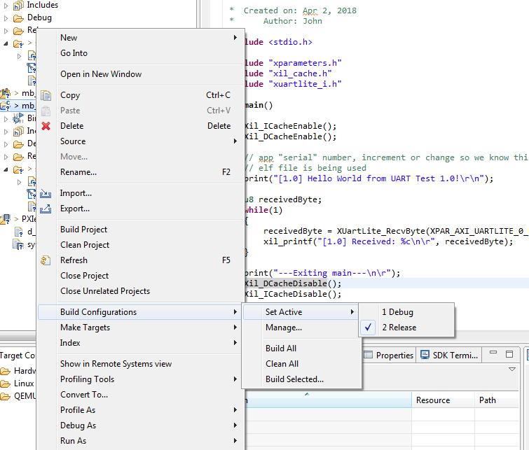
- I set the active configuration to Release for both projects. This isn’t really necessary for a small design such as this one, but it is a good habit to have.
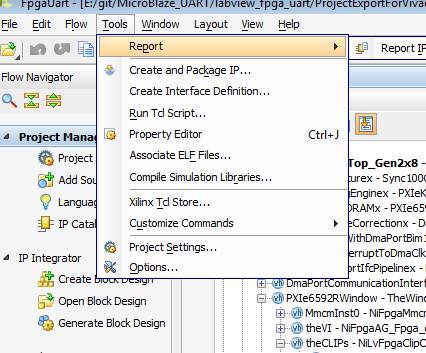
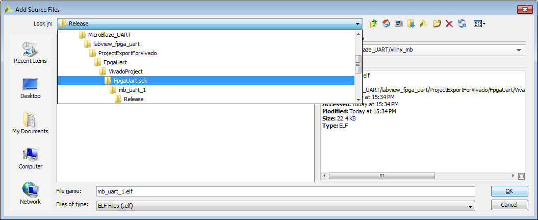
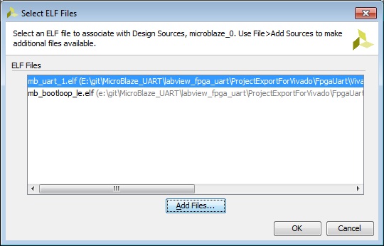
- Now we go back to Vivado and click “Tools->Associate ELF Files…”
- We do not have to select an elf file for simulation, but you can if you wish to create a test bench for this project. I have done this in the past and it takes me about 3 hours to simulate 100 milliseconds. With the method described on this page, it becomes much easier to just swap out the elf file and to regenerate the bitstream.
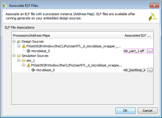
- We select the first elf file – “mb_uart_1.elf”
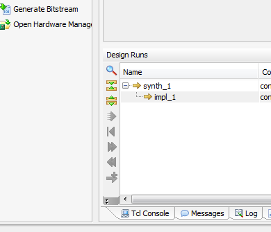
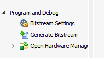
- And finally, we click on “Generate Bitstream”
Hi John,
Thankyou for an excellent tutorial. What do you do to get it all running in LabView after the bitstream is generated?
I’m contemplating trying to get an existing Linux based Microblaze system running on a Labview FPGA board but I’m thinking the size of the Linux OS system is going to need external DDR but maybe there’s enough BlockRAM. I’ll let you know if I make any progress.
Stuart