
I normally avoid shop words or “corporate speak” because I feel it dehumanizes us, but sometimes these phrases are necessary. So here is the “30,000 foot” view. And please pardon the appearance of my flow charts and diagrams, I am not a graphic designer…
All images open in a new tab, so just click on them with ease until I figure out how to make this WordPress theme wider.
Take look at this:
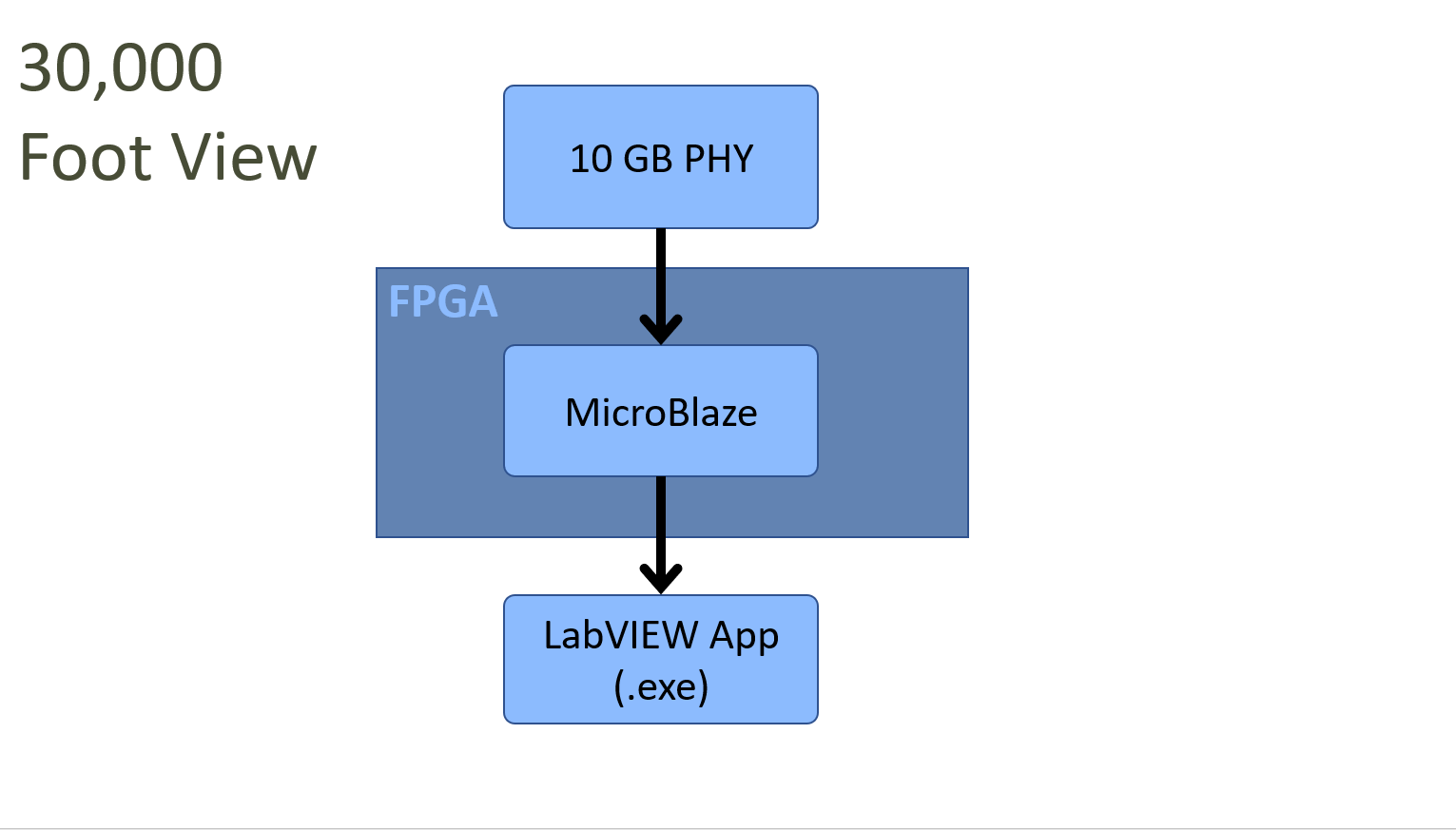
- There are four (4) 10 Gigabit ports available on this device, but I am using only one of them for this design.
- The FPGA design contains a MicroBlaze soft-core Processor
- This MicroBlaze soft-core Processor is connected to a LabVIEW for Windows Executable, which is the same thing as a standard .exe file.
Now some more details:
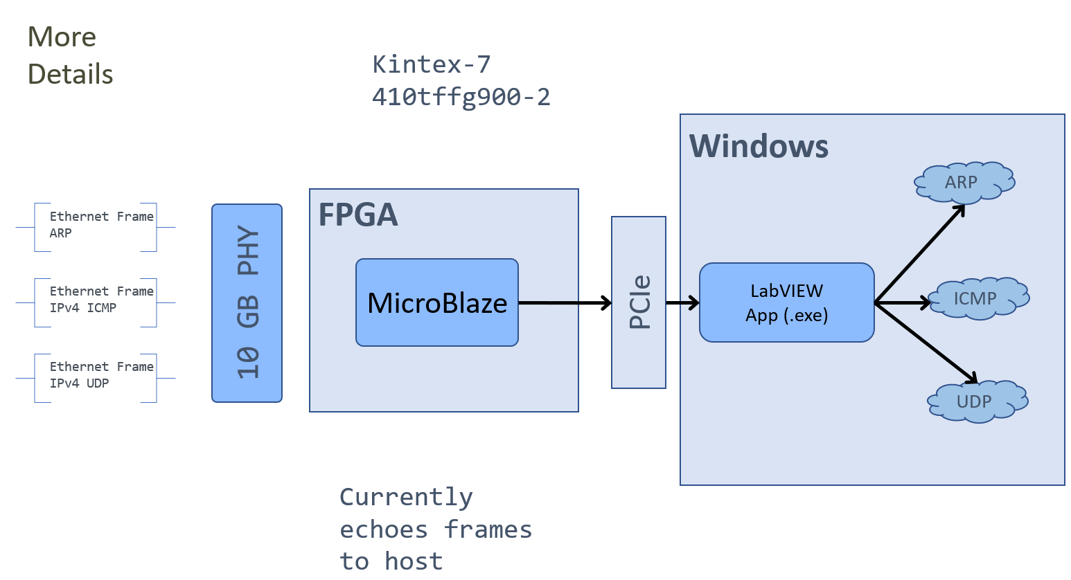
- Any type of Ethernet Frame can enter the 10 Gigabit PHY, as shown in the diagram:
- An Ethernet Frame with an ARP Request
- An Ethernet Frame with an IPv4 Packet containing an ICMP packet, otherwise known as a “Ping” message
- An Ethernet Frame with an IPv4 Packet containing a UDP packet. You may known this as “multicast” or “broadcast” messages.
And finally, everything, the full shebang:
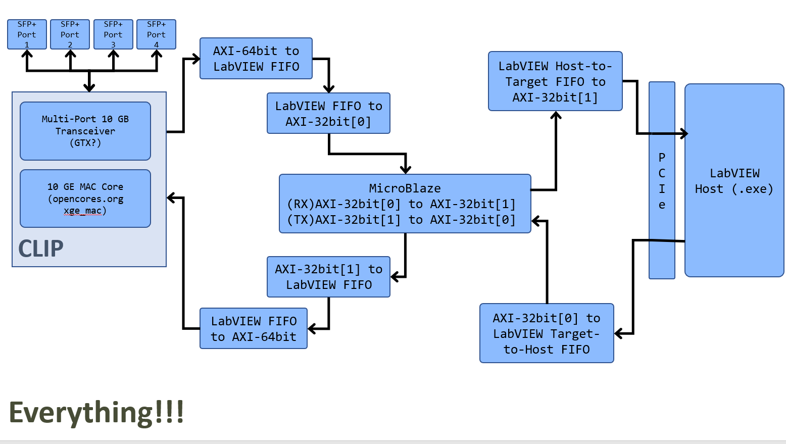 I have broken out the details of the hardware comprising the 10 Gigabit connection. Technically it consists of 4 SFP+ connectors going to a Multi-Gigabit Transceiver. Now normally I would think that there is some sort of chip in between the SFP+ and the FPGA, but I believe that National Instruments has used some Xilinx IP that handles this for us. See, I don’t even know what hardware is being used, but I am able to use it and make an FPGA-based Network Card!
The data from the Multi-Gigabit Transceiver then goes to the 10 GE MAC Core, which sends all received packets
First, a Definition
CLIP – Stands for Component Level IP and is a method of bringing in non-LabVIEW FPGA code in to LabVIEW. Basically you take a synthesized design, wrap it up in some VHDL and import this VHDL file to LabVIEW. In this case an instance of the OpenCores 10 GE Mac is being brought in to the the design.
See the top-level wrapper VHDL file here:
https://github.com/JohnStratoudakis/LabVIEW_Fpga/blob/master/07_10_Gigabit_CLIP/CLIP/TenGbEClip.vhd
See the source code of this core here:
See the official project website for this core here:
https://opencores.org/project,xge_mac
Now the Descriptions
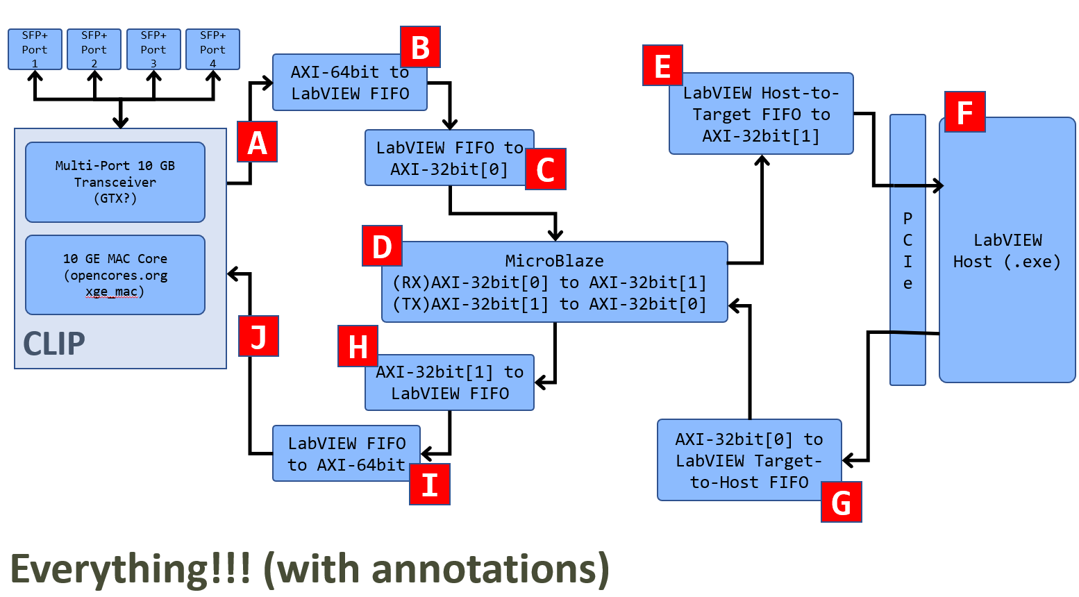
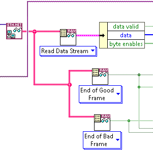
A – The reading of incoming frames is wrapped up in to a nice library by National Instruments, that even includes some IP to respond to ARP messages. I have stripped all of this usage out for this design because I wanted simplicity for learning. Anyway, on each clock cycle you have the following variables:
- data valid [boolean]
- data [64 bit WORD]
- byte enables [array of 8 booleans]
- End of Good Frame [boolean]
- End of Bad Frame [boolean]
Here is a screenshot of the usage for this, it should be very easy to understand once you have an idea of what LabVIEW is and how it works.
B – Now the data coming from the 10 Gigabit PHY contains 64-bit WORDs, and 2 booleans, one for a good frame, and one for a bad frame. Now I do not know how to configure and properly use a 64-bit AXI-Data Stream FIFO with a MicroBlaze processor, so I had to convert this data manually myself. It did not take long, in fact I documented this in my log where it took me 1 hour and 15 minutes to do this following the LabVIEW FPGA State Machine paradigm. Think of the LabVIEW FPGA State Machine paradigm or pattern as the absolute best of both worlds in terms of VHDL/Verilog and LabVIEW.
So, we have data coming in what I call “AXI-64bit format” and we have to convert it/write it to a LabVIEW FIFO. Here is a close-up of this code:
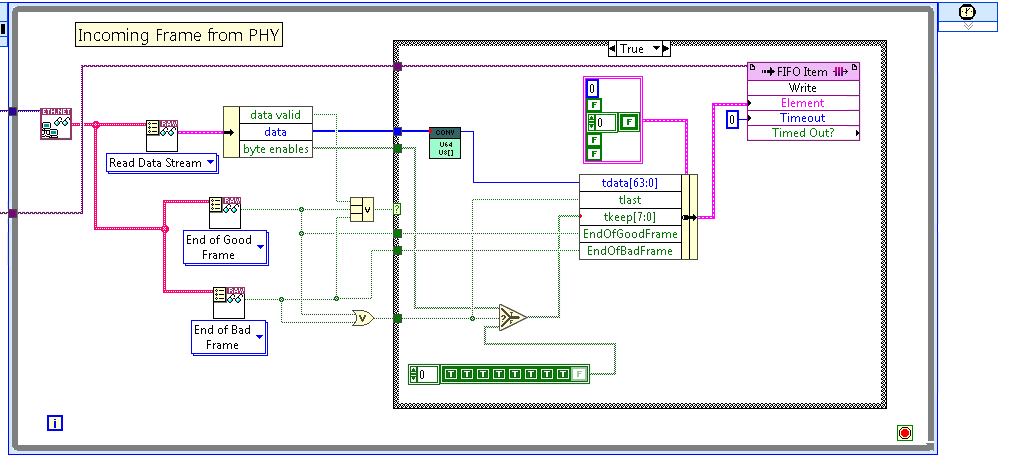
The code above is running inside a loop clocked at 156.25 MHz, and on the left is how we get the data from the 10 GE MAC. If “data valid”, or “End of Good Frame” or “End of Bad Frame” are true, we enter the self explanatory Case Structure, which is the same thing as an if statement. Inside this case we package all the data in to a custom “Cluster type”, which is the same thing as a C structure and write it in to a LabVIEW FIFO.
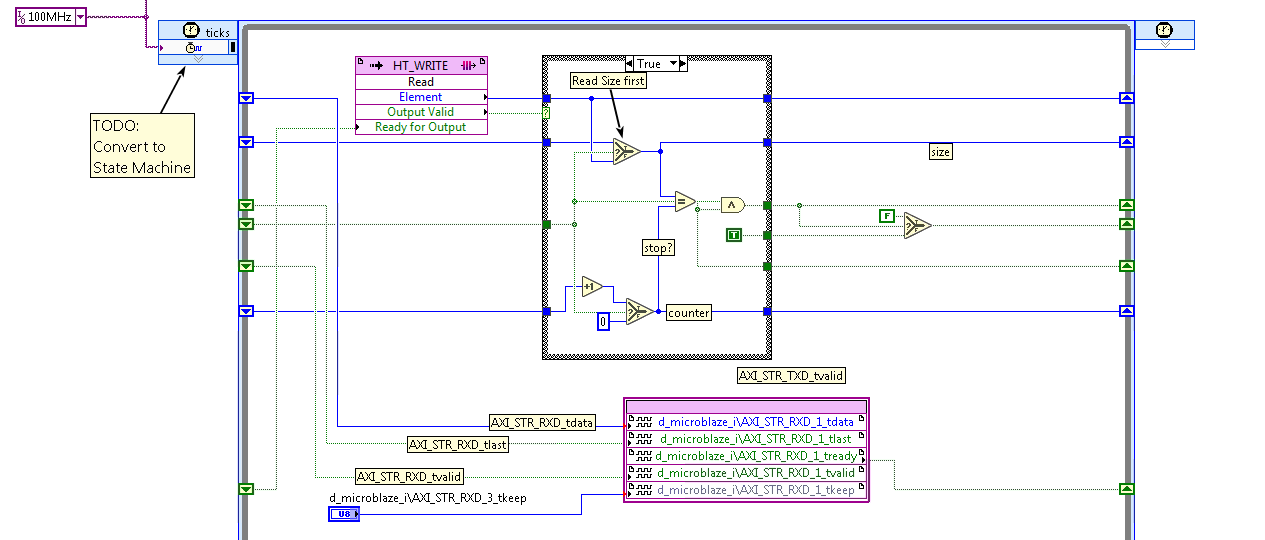
C – Now we read one element on each clock cycle of the custom LabVIEW Cluster defined in step B, and convert this in to a 32-bit AXI Data Stream to be read by the MicroBlaze.
Here is a screenshot of the entire loop, which runs at 100MHz, because I clocked my MicroBlaze to that speed. I could probably increase my MicroBlaze to 156.25MHz, but that will decrease my productivity in terms of longer synthesis times.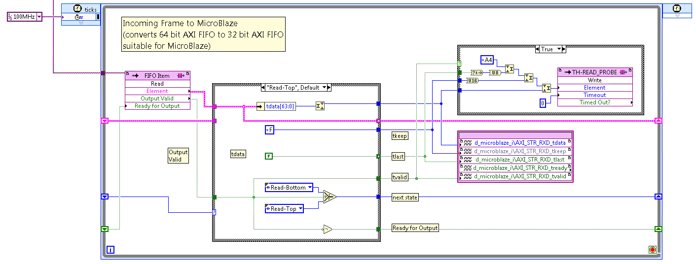
I zoomed out a bit further for this screenshot and included the clock specifier, which is 100 MHz. Also notice how there is another “Case Structure” inside this loop, but the case is not “True”, but it is a State Machine with the “Read-Top” case showing as the default state. This state checks if the incoming data is valid, and if so writes the upper 32 bits of the 64-bit data WORD in to the AXI-Data Stream FIFO that is connected to the MicroBlaze.
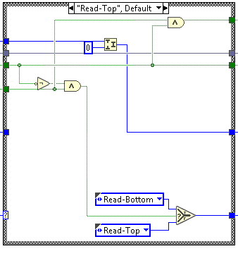
Here is a close-up of the “Read-Top” state:

Here is the other state:
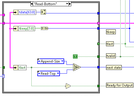
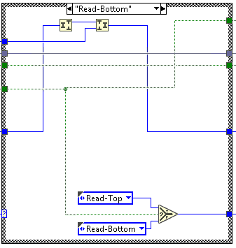
The “Read-Bottom” state. This state will write the lower half of the 64-bit WORD and will check if this is the final element in the Ethernet Frame. If this is the final element, it will enter the “Append-Size” state, which is incorrectly named, will fix that later “TODO: Rename Append-Size”. haha. Anyway, it will append some metadata indicating if this frame should be dropped or kept.
The final state – “Append-Size”:
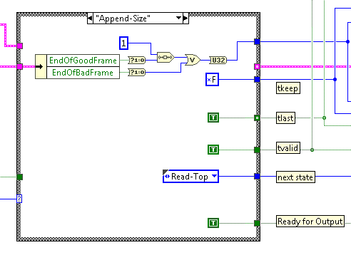
This code is very simple. I set TKEEP to all one’s, or 0b1111, and I set the first 2 bits of the 32-bit WORD to contain “End of Good Frame” and “End of Bad Frame”. Now why am I setting TKEEP to all 1’s? Well, simple, because I haven’t implemented this part yet, however, by setting it to all 1’s my code will still work because most TCP/IP stacks just ignore all padded 0’s.
D – Now the MicroBlaze has been programmed with a function that reads an incoming frame from AXI-Data Stream FIFO #0 and writes its contents to AXI-Data Stream FIFO #1. It also reads an incoming frame from AXI-Data Stream FIFO #1 and writes its contents to AXI-Data Stream FIFO #0. This is a simple passthrough that exercises my implementation of the FIFOs.
A direct link to the source code of this C code that is running in the MicroBlaze:
And a screenshot:

E – Now what happens after the source code above executes? Well, data is read from the 10 Gigabit PHY and read on the first AXI-Data Stream FIFO and written out back to the rest of the FPGA via the second AXI-Data Stream FIFO. So we want to read this ethernet frame and write it up to the Host application running on normal/regular Windows. This is very simple, read data, write data to a Target-to-Host LabVIEW FIFO, and if tlast is equal to true, include this in the metadata, which for now is simply the upper half of the 64-bit WORD.
F – Now how do you read this data on the host? Well, if you are familiar with LabVIEW, the code would look like this:
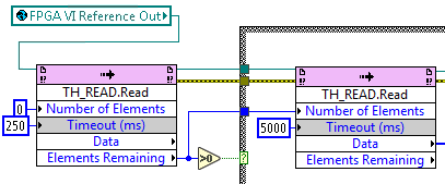
The green box contains a reference to the running FPGA. The first box on the left polls the FIFO to see if any elements are available, and if the number of elements available is greater than 0 it reads that number of elements.
If you wanted to do this from C++, you could use LabWindows CVI to read from the FPGA interface as such:
/* read the DMA FIFO */
NiFpga_MergeStatus(&status, NiFpga_ReadFifoI16 (session,
NiFpga_fpga_TargetToHostFifoI16_AIFIFO,
data, numSamples, timeout, &r));
(See: http://www.ni.com/tutorial/8638/en/)
Please note that you can also link to the LabWindows CVI library and use it from your existing C++ applications. Drivers for this specific board are only available for Windows, but if you are a big bank or financial firm with deep pockets, I’m sure you can set up some sort of agreement with National Instruments to port this code and drivers to <Operating System of your Choice>.
Okay, that is great, now what about writing data from the Host application back to the FPGA for sending out of the 10 Gigabit PHY? Well, you do the opposite, you enter the codes in reverse. (Spies Like Us).
Instead of a “Target-to-Host” FIFO, use a “Host-to-Target” FIFO, and in my case, I prepend the size in WORDs to the packet to be sent.
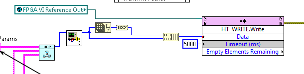
Again, the green box is a reference to the running FPGA. The square light green colored box is a function, also known as a “sub-VI” that I wrote that generates a UDP packet (or is it a UDP datagram? I forget). The output of this UDP packet is converted in to 32-bit WORDS by the box with a white background, and then the size is prepended to this array and written in to the “HT_WRITE” LabVIEW Host-to-Target FIFO.
G – So we are receiving data in the following format from the host:
<size>
<WORD1>
<WORD2>
…
<WORDN>
We read the size and then the rest of the elements from the FIFO and write them to the 2nd AXI-Data Stream FIFO that is connected to the MicroBlaze. Again note that I have not yet fully implemented the proper usage of the TKEEP signals, so in this case the TKEEP signal can be dynamically set from the Host application for testing purposes.
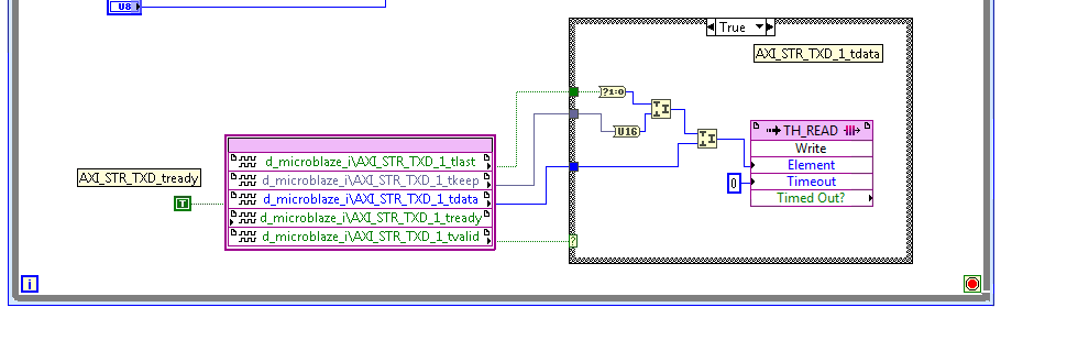
H – Now that the MicroBlaze has read our outgoing ethernet frame on Fifo #1 and has written the same outgoing frame on FIFO #0, we have to convert this 32-bit AXI Data Stream in to 64-bit words that are suitable for our 10 Gigabit Ethernet PHY.
This time however, I used a proper state machine and named all of the states correctly.
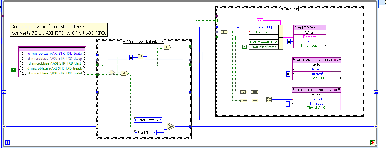
The left-most box connects the signals from the MicroBlaze to LabVIEW and wires them in to the state machine. If the data is valid and it is not the last element, the top half is stored in to a shift-register and the next state is “Read-Bottom”. Here is a close-up of the “Read-Top” state:
And here is a close-up of the “Read-Bottom” state:
I – Now we have written the 32-bit data coming from the MicroBlaze in to a LabVIEW FIFO with 64-bit data WORDS and we have to write this out using the CLIP, via the National Instruments provided wrapper.
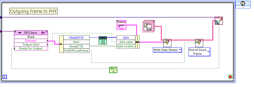
Look at how simple and beautiful this code is!
You can look at the source code here: (you must clone the repository to your local machine to see it easier, just clone it and open the 2nd file – the html file)
- FPGA top level
If you do now know git, you can also download a zip file of the entire repository:
https://github.com/JohnStratoudakis/LabVIEW_Fpga/archive/master.zip
If you somewhat know git, you can:
git clone git@github.com:JohnStratoudakis/LabVIEW_Fpga.git
And finally, browse the documentation, which is probably outdated here:
https://github.com/JohnStratoudakis/LabVIEW_Fpga/tree/master/07_10_Gigabit_CLIP
Up Next
So what now? Do I continue cleaning up the code and updating documentation? Do I make a youtube video demonstrating this? Do I modify the MicroBlaze code to no longer just be a “passthrough” but instead to send all data through the lwIP TCP/IP stack? If I do this, I will have to modify the elf file (compiled binary) that is embedded in to my design, breaking this design, so I can make multiple Xilinx checkpoints and it will work, but that will confuse all of my readers… Man decisions, decisions.
How about this, I finalize this project, make a new sub-directory in the source code and make a brand new LabVIEW FPGA project and this time I will use the lwIP version of the source code and I will make sure that everything is reproducible. It is raining now anyway and I want to stay inside and code…