
Now you can run LabVIEW FPGA on the hardware of your choice with the new “LabVIEW FPGA IP Export Utility”.
That sounds great, but what’s that got to do with me? (quoting Rambo 3)
Step 1 – Pick a non-National Instruments FPGA Board
You will have to pick a non-National Instruments FPGA board that has an FPGA that uses Vivado (7 Series devices and above) and has a corresponding LabVIEW FPGA board that uses a device of the same family. What does same family mean? Well, a Virtex-7 chip such as the VX485T has the same family as the VX690T.
If you want to run LabVIEW on other hardware, you will have to pay for and upgrade to the premium version of this tool which exports to VHDL source code. (This does not appear to be available yet, as per the documentation they request that you email them. As for me? I am happy with the encrypted netlist for now, because it keeps things simpler and will allow for easier licensing.)
For this post, I am going to select the NetFPGA-1G-CML Kinex-7 FPGA Development Board, which has a Xilinx Kintex-7 XC7K325T FPGA. See:
https://netfpga.org/site/#/systems/2netfpga-1g-cml/details/
Retails for $1,499.00
https://store.digilentinc.com/netfpga-sume-virtex-7-fpga-development-board/
Step 2 – Pick a Corresponding National Instruments Board
Now that you have selected the Xilinx FPGA Family that you want to use, now you have to select a National Instruments board that uses the same FPGA family, which means Kintex-7.
This page has a list of Xilinx FPGA’s and corresponding National Instruments Boards:
I will be selecting the PXIe-7868R board.
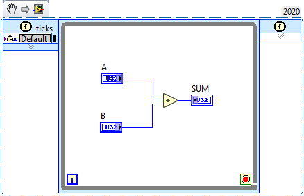
Step 3 – Create a LabVIEW Project using this board
Create a project with the PXIe-7858R board as one of its targets, and make a very simple top-level vi. Here is a very simple VI Snippet:
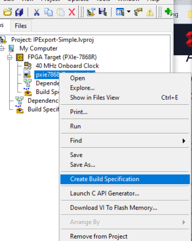
Step 4 – Create a Build Specification
Right-click on the top-level vi and select ‘Create Build Specification’
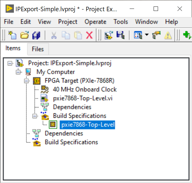
And after you should see:
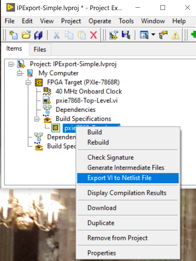
Step 5 – Create a Netlist Export
A new option is available under the right-click menu of the build specification called “Export to Netlist”
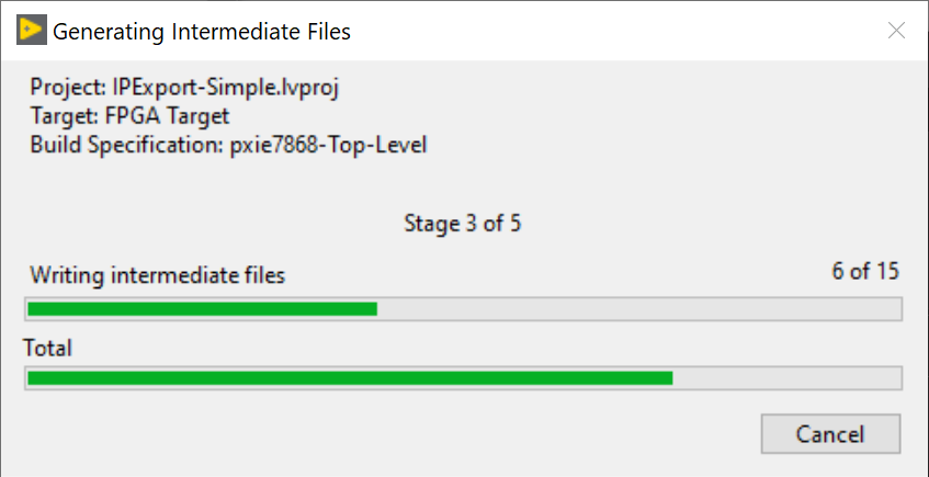
It runs the first steps that it normally does when you synthesize an FPGA project:
Be careful, the window just disappears and expects you to know where the netlist will be saved. (Hey, that’s much better than them sitting on it internally and not releasing it. And, this is one of those RTFM issues anyway…)
C:\NIFPGA\compilation\ipexport-simple_FPGATarget_<random text>
In my case, there is a Vivado Checkpoint file and a wrapper VHD file.
The code looks pretty cool. And remember the most important thing – ACTIVE HIGH!
NiFpgaIPWrapper_pxie7868_dash_Top_dash_Level.vhd
-- VHDL wrapper for NiFpgaAG_pxie7868_dash_Top_dash_Level-- Generated by LabVIEW FPGA IP Export Utility---- Ports:-- reset : Reset port. Minimum assertion length: 1 base clock cycles.-- Minimum de-assertion length: 40 base clock cycles.-- enable_in : Enable in port. Minimum re-initialization length: 7 base clock cycles.-- enable_out : Enable out port.-- enable_clr : Enable clear port.-- ctrlind_00_B : Top level control "B", sync to Clk40, u32-- ctrlind_01_A : Top level control "A", sync to Clk40, u32-- ctrlind_02_SUM : Top level indicator "SUM", sync to Clk40, u32-- Clk40 : Clock "40 MHz Onboard Clock", nominal frequency 40.00 MHz, base clock
library ieee;use ieee.std_logic_1164.all;
entity NiFpgaIPWrapper_pxie7868_dash_Top_dash_Level isport (reset : in std_logic;enable_in : in std_logic;enable_out : out std_logic;enable_clr : in std_logic;ctrlind_00_B : in std_logic_vector(31 downto 0);ctrlind_01_A : in std_logic_vector(31 downto 0);ctrlind_02_SUM : out std_logic_vector(31 downto 0);Clk40 : in std_logic);end NiFpgaIPWrapper_pxie7868_dash_Top_dash_Level;
architecture vhdl_labview of NiFpgaIPWrapper_pxie7868_dash_Top_dash_Level is
component NiFpgaAG_pxie7868_dash_Top_dash_Levelport (reset : in std_logic;enable_in : in std_logic;enable_out : out std_logic;enable_clr : in std_logic;ctrlind_00_B : in std_logic_vector(31 downto 0);ctrlind_01_A : in std_logic_vector(31 downto 0);ctrlind_02_SUM : out std_logic_vector(31 downto 0);Clk40 : in std_logic;tDiagramEnableOut : in std_logic);end component;
beginMyLabVIEWIP : NiFpgaAG_pxie7868_dash_Top_dash_Levelport map(reset => reset,enable_in => enable_in,enable_out => enable_out,enable_clr => enable_clr,ctrlind_00_B => ctrlind_00_B,ctrlind_01_A => ctrlind_01_A,ctrlind_02_SUM => ctrlind_02_SUM,Clk40 => Clk40,tDiagramEnableOut => '1');
end vhdl_labview;