So I am dealing with the following scenarios:
Scenario 1 – Genesys Zynq with SYZYGY SFP
I have the Genesys Zynq UltraScale+ MPSoC 3EG board that does not provide direct access to the PHY pins, but has a SYZYGY port that I have plugged in to the SZG-DUALSFP module with an SFP connector.
Scenario 2 – Arty A7 Artix-7 with 10/100 Mbit PHY
I have the Arty A7 Artx-7 FPGA Development Board that gives me direct access to the pins of a 10/100 Mbit PHY.
All I want to do is connect directly to a PHY so I can implement a LabVIEW based TCP/IP core, and as a starting Proof-of-Concept, I will take the already existing LabVIEW FPGA implementation (see their examples) and bring the UDP echo sample in.
So I create a design using the Arty board using a MicroBlaze processor, write a simple program and add an AXI Stream FIFO core and connect that to a custom verilog node that will hold the LabVIEW FPGA code. I do this because I want a way of communicating with the code running on the FPGA. The AXI Stream FIFO will bridge the LabVIEW FPGA code with the MicroBlaze processor, and what I will do is send some or all data received from the Ethernet PHY over the AXI Stream FIFO to a C++ application running on the MicroBlaze, and then via a UART connection that I make from my host computer to the Arty, see the results.
I can also use this as a way to properly figure out how to use the SZG-DUALSFP module as well.
Long story short, I add an AXI-Stream FIFO that is connected to a labview_ip node which will house my LabVIEW FPGA exported code. And for now I create a simple file that echoes a random packet of five 32-bit WORDS once per second.
Optimization Error
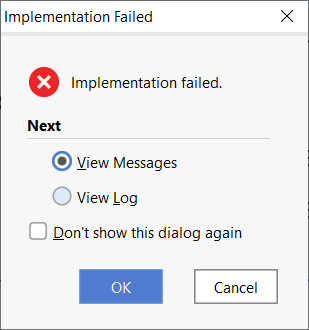
So I create this custom Verilog code, and click Generate Bitstream. After a few minutes I get the error mentioned in the title of this article. I originally had no idea how to debug this, but after some time on Xilinx Forums I figured it out… I forgot to wire up one value, and the design optimization removed it since it was unwired. Anyway, if you are using Vivado and you get this error, please continue…
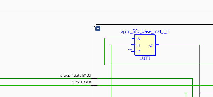
[Opt 31-67] Problem: A LUT3 cell in the design is missing a connection on input pin I2, which is used by the LUT equation. This pin has either been left unconnected in the design or the connection was removed due to the trimming of unused logic. The LUT cell name is: design_1_i/axi_fifo_mm_s_0/U0/COMP_IPIC2AXI_S/gtxd.COMP_TXD_FIFO/gfifo_gen.COMP_AXIS_FG_FIFO/COMP_FIFO/xpm_fifo_base_inst_i_1.
So the LUT cell name is:
design_1_i/axi_fifo_mm_s_0/U0/COMP_IPIC2AXI_S/gtxd.COMP_TXD_FIFO/gfifo_gen.COMP_AXIS_FG_FIFO/COMP_FIFO/xpm_fifo_base_inst_i_1
I manually run ‘Optimize Design’ with the the following commands:
set_param messaging.defaultLimit 100000
opt_design -verbose
(See: https://www.xilinx.com/support/answers/58616.html for more details on using this approach)
This reproduces the error, but the error appears in the TCL Console this time.
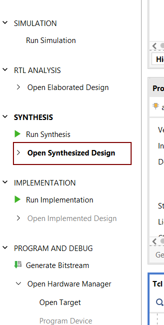
I open the Synthesized Design (‘Open Synthesized Design’ option on the left side-bar):
Show the object/cell by using the TCL console:
show_objects [ get_cells {design_1_i/axi_fifo_mm_s_0/U0/COMP_IPIC2AXI_S/gtxd.COMP_TXD_FIFO/gfifo_gen.COMP_AXIS_FG_FIFO/COMP_FIFO/xpm_fifo_base_inst_i_1}]
Which shows me this:
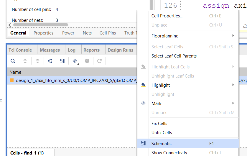
Then I go to the schematic by right-clicking on the cell and selecting ‘Schematic’:
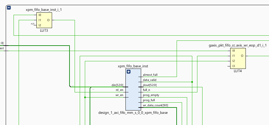
So this schematic shows that the signal I2 is unconnected. Now what is I2? I have no idea…
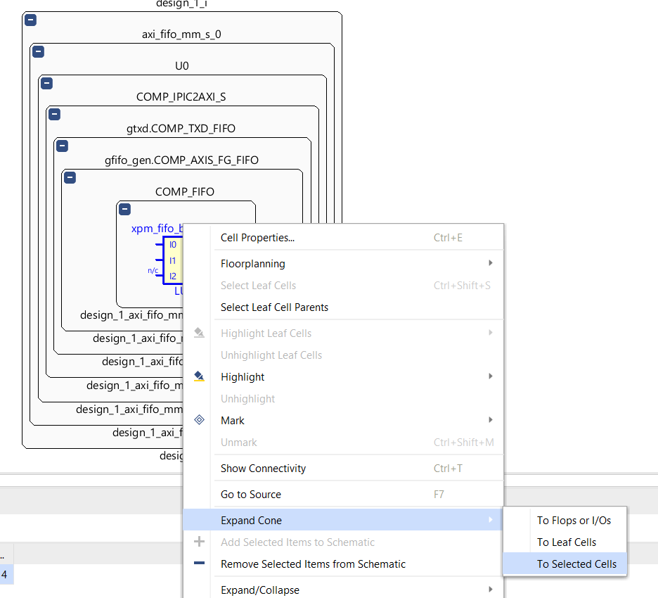
So I get more information by right-clicking and selecting ‘Expand Cone->To Selected Cells’:
The schematic will be pretty big, however the selected cell will be highlighted in blue and zoomed in like so:
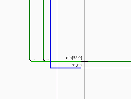
Then I follow the output wire until I find where it goes, notice that the wire is connected to ‘rd_en’, which sounds a lot like ‘Read Enable’ which is a port that the FIFO should have connected.
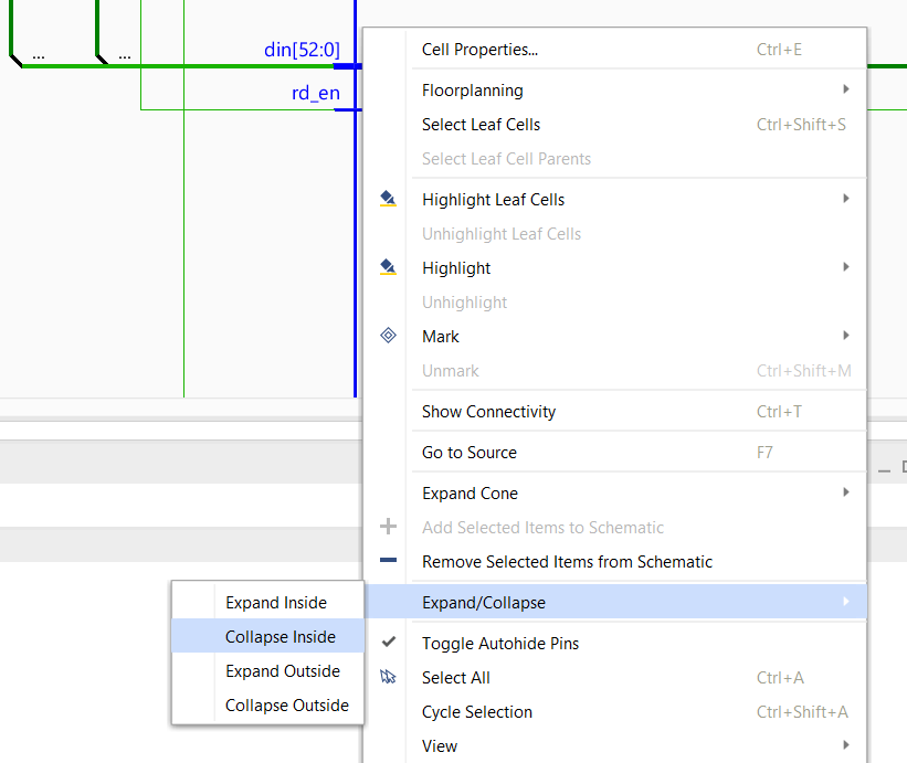
Now this might be too vague, so what if I wanted to know what component or cell the rd_en signal is going to? I right-click on the border of this cell/component and select ‘Expand/Collapse->Collapse Inside’:
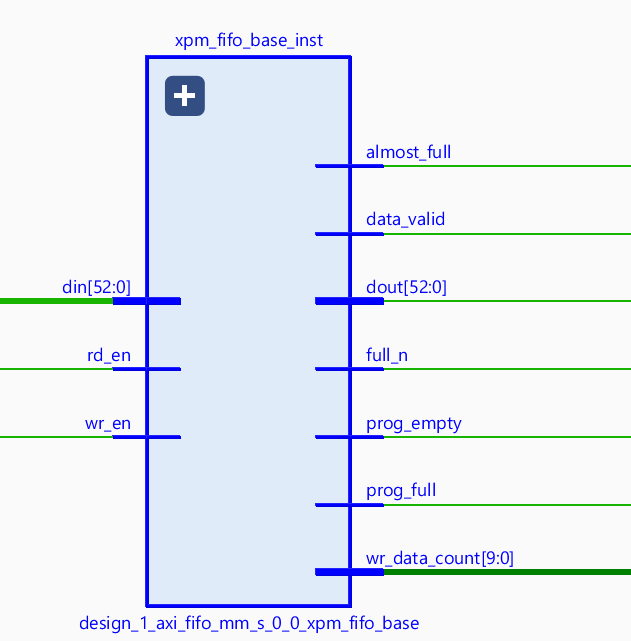
With this view, I know immediately what is wrong, I must have never wired the ready or ‘Ready for Input’ signal somewhere between the AXI-Stream FIFO and my custom IP.
And here is a slightly zoomed out view:
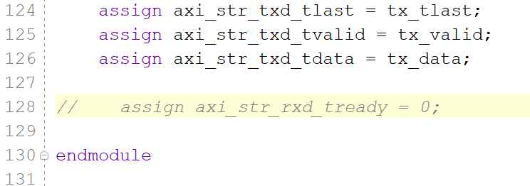
I go back to my Verilog code and realize that I never assigned a value to the ‘Transmit Ready’ signal – even though I would have expected this to work and to default to a value of 0.
For the curious, adding line 128 fixed the error:


